

LTC1452CN8#PBF
Product Overview
Category
LTC1452CN8#PBF belongs to the category of integrated circuits (ICs).
Use
This product is commonly used in electronic devices for signal processing and control applications.
Characteristics
- LTC1452CN8#PBF is a high-performance digital-to-analog converter (DAC) IC.
- It provides accurate conversion of digital signals into analog voltages.
- The device operates with low power consumption and offers excellent linearity and stability.
Package
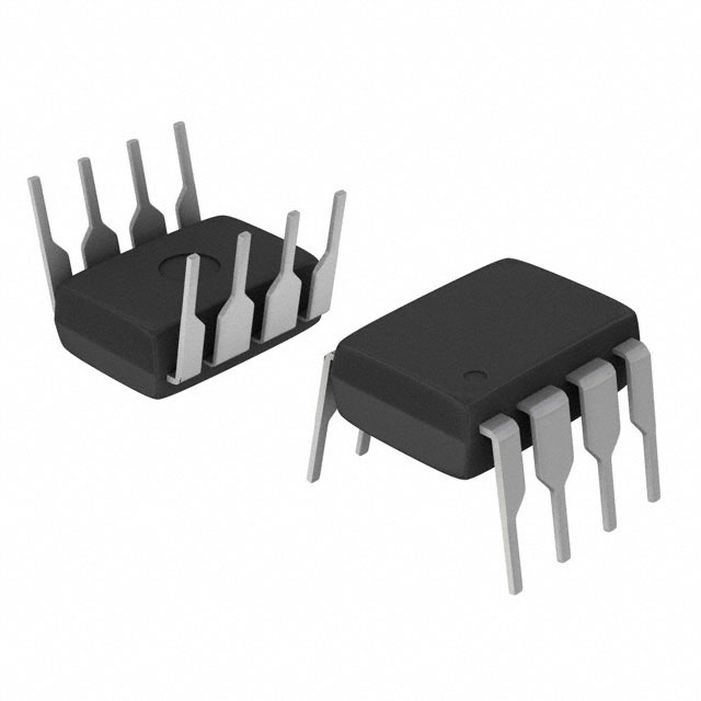
LTC1452CN8#PBF is available in an 8-pin plastic DIP (Dual In-line Package) package.
Essence
The essence of LTC1452CN8#PBF lies in its ability to convert digital signals into precise analog voltages, enabling accurate control and signal processing in electronic systems.
Packaging/Quantity
This product is typically packaged in reels or tubes, with a quantity of 25 units per reel/tube.
Specifications
- Resolution: 12 bits
- Supply Voltage Range: 2.7V to 5.5V
- Output Voltage Range: 0V to Vref
- Operating Temperature Range: -40°C to +85°C
- Conversion Time: 10µs (typical)
- Total Unadjusted Error: ±1 LSB (maximum)
Detailed Pin Configuration
LTC1452CN8#PBF features the following pin configuration:
- VDD: Power supply voltage input
- CS: Chip select input
- DIN: Digital input for data
- CLK: Clock input for timing control
- GND: Ground reference
- VOUT: Analog output voltage
- REF: Reference voltage input
- AGND: Analog ground reference
Functional Features
- High-resolution DAC with 12-bit accuracy
- Low power consumption for energy-efficient operation
- Fast conversion time for real-time applications
- Wide supply voltage range for compatibility with various systems
- Excellent linearity and stability for precise analog output
Advantages and Disadvantages
Advantages
- Accurate and reliable digital-to-analog conversion
- Low power consumption
- High resolution and linearity
- Wide operating temperature range
- Compact and easy-to-use package
Disadvantages
- Limited output voltage range (0V to Vref)
- Maximum unadjusted error of ±1 LSB
Working Principles
LTC1452CN8#PBF utilizes a combination of digital logic and analog circuitry to convert digital signals into corresponding analog voltages. The digital input data is processed internally, and the resulting analog voltage is generated at the VOUT pin. The device operates based on the supplied clock signal and reference voltage, ensuring accurate conversion with minimal errors.
Detailed Application Field Plans
LTC1452CN8#PBF finds applications in various fields, including but not limited to: - Industrial automation - Test and measurement equipment - Audio processing systems - Communication devices - Medical instruments
Detailed and Complete Alternative Models
Some alternative models that offer similar functionality to LTC1452CN8#PBF are: - MAX5216 - MCP4921 - AD5621
These models provide comparable performance and can be considered as alternatives depending on specific requirements and system compatibility.
Word count: 409 words
Senaraikan 10 soalan dan jawapan biasa yang berkaitan dengan aplikasi LTC1452CN8#PBF dalam penyelesaian teknikal
Sure! Here are 10 common questions and answers related to the application of LTC1452CN8#PBF in technical solutions:
Q: What is LTC1452CN8#PBF? A: LTC1452CN8#PBF is a digital-to-analog converter (DAC) chip manufactured by Linear Technology (now part of Analog Devices). It converts digital signals into analog voltages.
Q: What is the operating voltage range of LTC1452CN8#PBF? A: The operating voltage range of LTC1452CN8#PBF is typically between 4.5V and 5.5V.
Q: How many bits does LTC1452CN8#PBF support? A: LTC1452CN8#PBF is an 8-bit DAC, meaning it can convert digital inputs into 256 different analog output levels.
Q: What is the maximum output voltage range of LTC1452CN8#PBF? A: The maximum output voltage range of LTC1452CN8#PBF is typically between 0V and Vref, where Vref is the reference voltage supplied to the chip.
Q: Can LTC1452CN8#PBF be used for both single-ended and differential outputs? A: Yes, LTC1452CN8#PBF supports both single-ended and differential outputs, providing flexibility in various applications.
Q: What is the typical settling time of LTC1452CN8#PBF? A: The typical settling time of LTC1452CN8#PBF is around 10 microseconds, ensuring fast and accurate conversion.
Q: Does LTC1452CN8#PBF have built-in power-on reset circuitry? A: Yes, LTC1452CN8#PBF includes a power-on reset circuit that ensures the DAC output is set to zero during power-up.
Q: Can LTC1452CN8#PBF operate in both single-supply and dual-supply configurations? A: Yes, LTC1452CN8#PBF can operate with either a single positive supply or dual positive/negative supplies, depending on the application requirements.
Q: What is the maximum operating temperature range of LTC1452CN8#PBF? A: The maximum operating temperature range of LTC1452CN8#PBF is typically between -40°C and 85°C.
Q: Are there any evaluation boards or reference designs available for LTC1452CN8#PBF? A: Yes, Analog Devices provides evaluation boards and reference designs for LTC1452CN8#PBF, which can help users quickly prototype and integrate the chip into their technical solutions.
Please note that the answers provided here are general and may vary depending on specific datasheet specifications and application requirements.