

MAX533BEEE+T
Product Overview
- Category: Integrated Circuit (IC)
- Use: Digital-to-Analog Converter (DAC)
- Characteristics: High precision, low power consumption
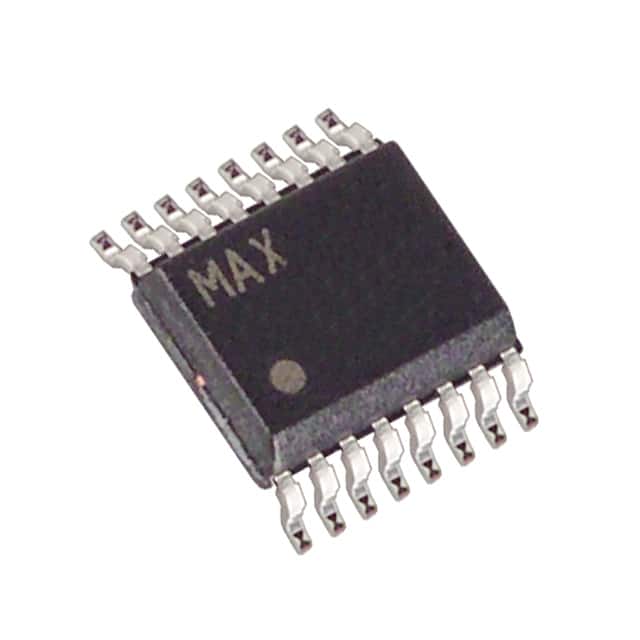
- Package: 16-pin TSSOP (Thin Shrink Small Outline Package)
- Essence: Converts digital signals into analog voltage outputs
- Packaging/Quantity: Tape and reel packaging, quantity per reel varies
Specifications
- Resolution: 12 bits
- Number of Channels: 1
- Supply Voltage Range: 2.7V to 5.5V
- Output Voltage Range: 0V to Vref
- Operating Temperature Range: -40°C to +85°C
- DNL (Differential Non-Linearity): ±0.5 LSB (Least Significant Bit)
- INL (Integral Non-Linearity): ±1 LSB
- Power Consumption: 0.4mW (typical)
Pin Configuration
The MAX533BEEE+T has a total of 16 pins, each serving a specific function:
- VDD: Positive supply voltage
- AGND: Analog ground
- REF: Reference voltage input
- VOUT: Analog output voltage
- DGND: Digital ground
- DIN: Serial data input
- SCLK: Serial clock input
- CS: Chip select input
- LDAC: Load DAC input
- SHDN: Shutdown control input
- NC: No connection
- NC: No connection
- NC: No connection
- NC: No connection
- NC: No connection
- VSS: Negative supply voltage
Functional Features
- High-resolution DAC with 12-bit output
- Low power consumption for energy-efficient applications
- Serial interface for easy integration with microcontrollers
- Shutdown control for power-saving mode
- Load DAC input for simultaneous update of multiple DACs
Advantages and Disadvantages
Advantages
- High precision output with low DNL and INL
- Wide supply voltage range allows flexibility in system design
- Small package size enables space-saving PCB layout
- Serial interface simplifies communication with other devices
Disadvantages
- Limited to single-channel output
- Requires external reference voltage for accurate conversion
- Not suitable for applications requiring higher resolution
Working Principles
The MAX533BEEE+T is a digital-to-analog converter that converts digital signals into analog voltage outputs. It utilizes a 12-bit resolution to provide precise analog voltage levels. The device operates by accepting serial data input (DIN) and clock input (SCLK) to convert the digital information into an analog output voltage (VOUT). The reference voltage (REF) determines the maximum output voltage, which can be adjusted according to the application requirements.
Detailed Application Field Plans
The MAX533BEEE+T finds applications in various fields, including:
- Industrial Automation: Control systems, process monitoring, and instrumentation.
- Audio Equipment: Digital audio processing, volume control, and equalization.
- Test and Measurement: Signal generation, waveform synthesis, and calibration.
- Communication Systems: Baseband signal processing, modulation, and demodulation.
- Automotive Electronics: Sensor calibration, actuator control, and engine management.
Detailed and Complete Alternative Models
- MAX5312BCPD+: 12-bit DAC with dual channels and internal reference voltage.
- MCP4922-E/P: 12-bit DAC with dual channels and SPI interface.
- AD5620BRJZ-2500RL7: 12-bit DAC with single channel and I2C interface.
- LTC2630ACSC6-LM12#TRMPBF: 12-bit DAC with single channel and rail-to-rail output.
- DAC8412FPCZ-REEL7: 12-bit DAC with dual channels and parallel interface.
These alternative models offer similar functionality and can be considered based on specific application requirements.
Word count: 525 words
Senaraikan 10 soalan dan jawapan biasa yang berkaitan dengan aplikasi MAX533BEEE+T dalam penyelesaian teknikal
Sure! Here are 10 common questions and answers related to the application of MAX533BEEE+T in technical solutions:
1. What is the MAX533BEEE+T? The MAX533BEEE+T is a digital-to-analog converter (DAC) IC manufactured by Maxim Integrated. It converts digital signals into analog voltages.
2. What is the voltage range of the MAX533BEEE+T? The MAX533BEEE+T has a voltage output range of 0V to VREF, where VREF is the reference voltage provided externally.
3. How many bits does the MAX533BEEE+T have? The MAX533BEEE+T is a 12-bit DAC, meaning it can convert digital signals into 4096 different analog voltage levels.
4. What is the supply voltage range for the MAX533BEEE+T? The supply voltage range for the MAX533BEEE+T is typically between 2.7V and 5.5V.
5. What is the typical power consumption of the MAX533BEEE+T? The typical power consumption of the MAX533BEEE+T is around 0.5mW.
6. Can the MAX533BEEE+T be used in both single-ended and differential mode? Yes, the MAX533BEEE+T can be used in both single-ended and differential mode, depending on the application requirements.
7. Does the MAX533BEEE+T have an internal voltage reference? No, the MAX533BEEE+T does not have an internal voltage reference. An external reference voltage needs to be provided.
8. What is the maximum settling time of the MAX533BEEE+T? The maximum settling time of the MAX533BEEE+T is typically 10µs.
9. Can the MAX533BEEE+T be used in industrial applications? Yes, the MAX533BEEE+T is suitable for use in various industrial applications, including process control, automation, and instrumentation.
10. What is the package type of the MAX533BEEE+T? The MAX533BEEE+T is available in an SOIC-16 package, which stands for Small Outline Integrated Circuit with 16 pins.
Please note that the answers provided here are general and may vary depending on the specific datasheet and application requirements.