

MAX5423ETA+T
Product Overview
- Category: Integrated Circuit (IC)
- Use: Digital-to-Analog Converter (DAC)
- Characteristics: High precision, low power consumption
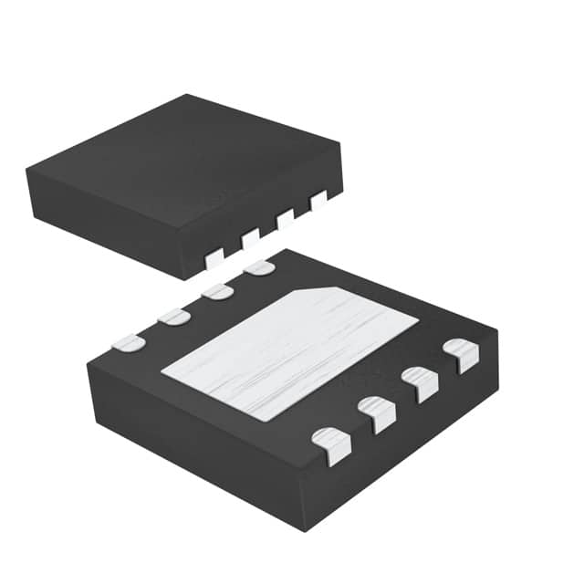
- Package: 8-pin TDFN (Thin Dual Flat No-Lead) package
- Essence: Converts digital signals into analog voltage or current
- Packaging/Quantity: Tape and reel packaging, available in quantities of 2500 units per reel
Specifications
- Resolution: 12 bits
- Supply Voltage Range: 2.7V to 5.5V
- Output Voltage Range: 0V to Vref
- Operating Temperature Range: -40°C to +85°C
- Total Unadjusted Error: ±1 LSB (Least Significant Bit)
- Power Consumption: 0.5mW (typical)
Pin Configuration
The MAX5423ETA+T has the following pin configuration:
```
| | --|VDD VREF|-- --|GND CS |-- --|SCLK DIN |-- --|SDO AGND|-- --|OUT AGND|-- --|AGND AGND|-- --|AGND AGND|-- |___________| ```
Functional Features
- High accuracy and linearity
- Low glitch impulse
- Fast settling time
- Serial interface for easy integration with microcontrollers
- Power-on reset function
- Software programmable output range
Advantages and Disadvantages
Advantages: - High precision conversion - Low power consumption - Small form factor - Easy integration with microcontrollers
Disadvantages: - Limited output voltage range - Requires external voltage reference
Working Principles
The MAX5423ETA+T is a digital-to-analog converter that converts digital signals into analog voltage or current. It utilizes a 12-bit resolution to provide high precision conversion. The device operates by receiving digital input data through the serial interface and converting it into an analog output voltage or current based on the supplied reference voltage. The MAX5423ETA+T also features a power-on reset function that ensures proper initialization upon power-up.
Detailed Application Field Plans
The MAX5423ETA+T is commonly used in various applications, including:
- Industrial automation: Control systems requiring precise analog outputs.
- Test and measurement equipment: Generating accurate analog signals for testing purposes.
- Audio equipment: Digital-to-analog conversion for audio signal processing.
- Communication systems: Generating analog signals for modulation and demodulation processes.
- Medical devices: Precise control of analog signals in medical equipment.
Detailed and Complete Alternative Models
- MAX5424ETA+T: Similar specifications with an extended temperature range (-40°C to +125°C).
- MAX5425ETA+T: Higher resolution (14 bits) with similar characteristics and package.
Note: This is not an exhaustive list, and there may be other alternative models available from different manufacturers.
This entry provides an overview of the MAX5423ETA+T, including its product category, use, characteristics, package, specifications, pin configuration, functional features, advantages and disadvantages, working principles, detailed application field plans, and alternative models.
Senaraikan 10 soalan dan jawapan biasa yang berkaitan dengan aplikasi MAX5423ETA+T dalam penyelesaian teknikal
Sure! Here are 10 common questions and answers related to the application of MAX5423ETA+T in technical solutions:
Q: What is the MAX5423ETA+T? A: The MAX5423ETA+T is a digital-to-analog converter (DAC) IC that converts digital signals into analog voltage outputs.
Q: What is the operating voltage range of the MAX5423ETA+T? A: The MAX5423ETA+T operates within a voltage range of 2.7V to 5.5V.
Q: How many bits of resolution does the MAX5423ETA+T have? A: The MAX5423ETA+T has 14 bits of resolution, allowing for precise analog output control.
Q: What is the typical output voltage range of the MAX5423ETA+T? A: The typical output voltage range of the MAX5423ETA+T is 0V to VREF, where VREF is the reference voltage supplied to the DAC.
Q: Can the MAX5423ETA+T be used in both single-ended and differential output configurations? A: Yes, the MAX5423ETA+T can be configured for both single-ended and differential output modes, providing flexibility in various applications.
Q: Does the MAX5423ETA+T support I2C communication interface? A: Yes, the MAX5423ETA+T supports I2C serial interface, making it easy to integrate with microcontrollers and other digital systems.
Q: What is the maximum settling time of the MAX5423ETA+T? A: The maximum settling time of the MAX5423ETA+T is typically 10µs, ensuring fast response times for dynamic applications.
Q: Can the MAX5423ETA+T operate in a power-down mode? A: Yes, the MAX5423ETA+T has a power-down mode that reduces power consumption when the device is not in use.
Q: What is the temperature range for the MAX5423ETA+T? A: The MAX5423ETA+T can operate within a temperature range of -40°C to +85°C, making it suitable for a wide range of environments.
Q: Are there any evaluation boards or development kits available for the MAX5423ETA+T? A: Yes, Maxim Integrated provides evaluation kits and reference designs for the MAX5423ETA+T, which can help streamline the development process.
Please note that these answers are general and may vary depending on specific application requirements and datasheet specifications.