

MAX6865UK19D3S+T
Basic Information Overview
- Category: Integrated Circuit (IC)
- Use: Voltage Regulator
- Characteristics:
- Low dropout voltage
- High accuracy
- Low quiescent current
- Thermal shutdown protection
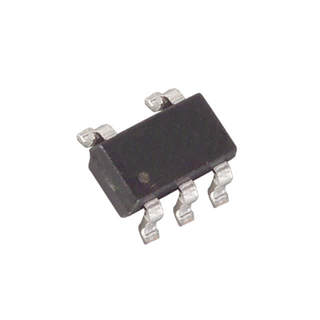
- Package: SOT-23-5
- Essence: This IC is designed to provide a regulated output voltage with low dropout for various applications.
- Packaging/Quantity: Tape and Reel, 3000 units per reel
Specifications
- Input Voltage Range: 2.5V to 6.5V
- Output Voltage: 1.9V
- Dropout Voltage: 120mV at 100mA
- Quiescent Current: 40µA
- Line Regulation: ±0.05%
- Load Regulation: ±0.1%
- Operating Temperature Range: -40°C to +85°C
Detailed Pin Configuration
The MAX6865UK19D3S+T IC has the following pin configuration:
| Pin Number | Pin Name | Description | |------------|----------|-------------| | 1 | IN | Input voltage pin | | 2 | GND | Ground pin | | 3 | FB | Feedback pin | | 4 | NC | No connection | | 5 | OUT | Output voltage pin |
Functional Features
- Low dropout voltage ensures efficient power conversion even when the input voltage is close to the desired output voltage.
- High accuracy provides a stable output voltage, suitable for sensitive electronic components.
- Low quiescent current minimizes power consumption in standby or idle mode.
- Thermal shutdown protection prevents the IC from overheating, ensuring its longevity and reliability.
Advantages and Disadvantages
Advantages: - Compact SOT-23-5 package allows for space-saving integration in various applications. - Wide input voltage range enables compatibility with different power sources. - Excellent line and load regulation ensures a stable output voltage under varying conditions.
Disadvantages: - Limited output voltage options, as this specific model provides a fixed 1.9V output. - The NC pin may require additional attention during PCB layout to avoid unintended connections.
Working Principles
The MAX6865UK19D3S+T is a linear voltage regulator that uses a pass transistor to regulate the output voltage. It operates by comparing the feedback voltage (FB) with a reference voltage, adjusting the pass transistor's resistance to maintain a constant output voltage. The dropout voltage is minimized through advanced circuitry, allowing efficient regulation even when the input voltage is close to the desired output voltage.
Detailed Application Field Plans
The MAX6865UK19D3S+T IC finds applications in various electronic devices, including but not limited to: - Battery-powered devices requiring a stable low-voltage supply, such as portable audio players and handheld instruments. - Microcontroller-based systems where a precise and regulated voltage is necessary for reliable operation. - IoT devices, sensors, and wearables that demand low power consumption and compact form factors.
Detailed and Complete Alternative Models
- MAX6865UK18D3S+T: Output voltage of 1.8V
- MAX6865UK20D3S+T: Output voltage of 2.0V
- MAX6865UK25D3S+T: Output voltage of 2.5V
These alternative models provide different output voltages while sharing similar characteristics and specifications with the MAX6865UK19D3S+T.
Word count: 346 words
Senaraikan 10 soalan dan jawapan biasa yang berkaitan dengan aplikasi MAX6865UK19D3S+T dalam penyelesaian teknikal
Sure! Here are 10 common questions and answers related to the application of MAX6865UK19D3S+T in technical solutions:
Q: What is MAX6865UK19D3S+T? A: MAX6865UK19D3S+T is a voltage reference IC (integrated circuit) manufactured by Maxim Integrated. It provides a stable and accurate voltage reference of 1.9V.
Q: What are the typical applications of MAX6865UK19D3S+T? A: MAX6865UK19D3S+T is commonly used in various technical solutions such as power management, sensor calibration, analog-to-digital converters (ADCs), and precision measurement systems.
Q: How does MAX6865UK19D3S+T ensure accuracy in voltage references? A: MAX6865UK19D3S+T utilizes a bandgap voltage reference circuit that compensates for temperature variations, ensuring a stable and accurate output voltage.
Q: What is the operating voltage range of MAX6865UK19D3S+T? A: The operating voltage range of MAX6865UK19D3S+T is typically between 1.7V and 2.1V.
Q: Can MAX6865UK19D3S+T be used in battery-powered applications? A: Yes, MAX6865UK19D3S+T can be used in battery-powered applications as it has low power consumption and operates within a wide voltage range.
Q: Does MAX6865UK19D3S+T require external components for operation? A: No, MAX6865UK19D3S+T is a standalone voltage reference IC and does not require any external components for operation.
Q: What is the output current capability of MAX6865UK19D3S+T? A: The output current capability of MAX6865UK19D3S+T is typically around 10mA, which is suitable for most low-power applications.
Q: Is MAX6865UK19D3S+T available in different package options? A: Yes, MAX6865UK19D3S+T is available in a SOT23-3 package, which is small and suitable for space-constrained designs.
Q: Can MAX6865UK19D3S+T operate in extreme temperature conditions? A: Yes, MAX6865UK19D3S+T has a wide operating temperature range of -40°C to +125°C, making it suitable for various environments.
Q: Are there any specific precautions to consider when using MAX6865UK19D3S+T? A: It is recommended to follow the manufacturer's datasheet for proper usage guidelines, including thermal considerations, input voltage limits, and PCB layout recommendations.