

ATF1508AS-10QC100
Product Overview
Category
ATF1508AS-10QC100 belongs to the category of programmable logic devices (PLDs).
Use
This product is primarily used in digital circuit design and implementation. It provides a flexible and customizable solution for various applications.
Characteristics
- Programmable: The ATF1508AS-10QC100 can be programmed to perform specific functions based on user requirements.
- High Integration: It integrates multiple logic gates, flip-flops, and other components into a single device, reducing the need for external components.
- Versatile: This PLD supports a wide range of applications due to its programmability.
- Low Power Consumption: The ATF1508AS-10QC100 is designed to operate efficiently with low power consumption.
- Fast Operation: It offers high-speed performance, enabling quick execution of complex logic operations.
Package
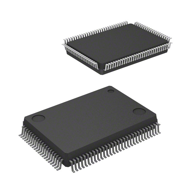
The ATF1508AS-10QC100 comes in a Quad Flat Package (QFP) with 100 pins.
Essence
The essence of ATF1508AS-10QC100 lies in its ability to provide reconfigurable logic functions, allowing designers to implement custom digital circuits without the need for dedicated hardware.
Packaging/Quantity
This product is typically packaged in reels or trays, with each reel or tray containing a specific quantity of ATF1508AS-10QC100 devices.
Specifications
- Device Type: ATF1508AS-10QC100
- Logic Cells: 1508
- Speed Grade: -10
- Operating Voltage: 3.3V
- I/O Pins: 100
- Maximum Frequency: 100 MHz
- Package Type: QFP
Detailed Pin Configuration
The ATF1508AS-10QC100 has 100 pins arranged as follows:
- Pin 1: VCCIO
- Pin 2: GND
- Pin 3: IO0
- Pin 4: IO1
- Pin 5: IO2
- Pin 6: IO3
- Pin 7: IO4
- Pin 8: IO5
- Pin 9: IO6
- Pin 10: IO7
- Pin 11: IO8
- Pin 12: IO9
- Pin 13: IO10
- Pin 14: IO11
- Pin 15: IO12
- Pin 16: IO13
- Pin 17: IO14
- Pin 18: IO15
- Pin 19: IO16
- Pin 20: IO17
- Pin 21: IO18
- Pin 22: IO19
- Pin 23: IO20
- Pin 24: IO21
- Pin 25: IO22
- Pin 26: IO23
- Pin 27: IO24
- Pin 28: IO25
- Pin 29: IO26
- Pin 30: IO27
- Pin 31: IO28
- Pin 32: IO29
- Pin 33: IO30
- Pin 34: IO31
- Pin 35: IO32
- Pin 36: IO33
- Pin 37: IO34
- Pin 38: IO35
- Pin 39: IO36
- Pin 40: IO37
- Pin 41: IO38
- Pin 42: IO39
- Pin 43: IO40
- Pin 44: IO41
- Pin 45: IO42
- Pin 46: IO43
- Pin 47: IO44
- Pin 48: IO45
- Pin 49: IO46
- Pin 50: IO47
- Pin 51: IO48
- Pin 52: IO49
- Pin 53: IO50
- Pin 54: IO51
- Pin 55: IO52
- Pin 56: IO53
- Pin 57: IO54
- Pin 58: IO55
- Pin 59: IO56
- Pin 60: IO57
- Pin 61: IO58
- Pin 62: IO59
- Pin 63: IO60
- Pin 64: IO61
- Pin 65: IO62
- Pin 66: IO63
- Pin 67: IO64
- Pin 68: IO65
- Pin 69: IO66
- Pin 70: IO
Senaraikan 10 soalan dan jawapan biasa yang berkaitan dengan aplikasi ATF1508AS-10QC100 dalam penyelesaian teknikal
Sure! Here are 10 common questions and answers related to the application of ATF1508AS-10QC100 in technical solutions:
Q: What is ATF1508AS-10QC100? A: ATF1508AS-10QC100 is a specific model of Field-Programmable Gate Array (FPGA) manufactured by Microchip Technology Inc.
Q: What are the key features of ATF1508AS-10QC100? A: Some key features of ATF1508AS-10QC100 include 1500 usable gates, 8 macrocells, 8 inputs/outputs, and a maximum operating frequency of 10 MHz.
Q: How can ATF1508AS-10QC100 be used in technical solutions? A: ATF1508AS-10QC100 can be used for various applications such as digital logic design, prototyping, system integration, and control systems.
Q: What programming languages can be used with ATF1508AS-10QC100? A: ATF1508AS-10QC100 can be programmed using Hardware Description Languages (HDLs) like VHDL or Verilog.
Q: Can ATF1508AS-10QC100 be reprogrammed after initial configuration? A: Yes, ATF1508AS-10QC100 is a reprogrammable FPGA, allowing for multiple configurations during its lifetime.
Q: What tools are required to program ATF1508AS-10QC100? A: To program ATF1508AS-10QC100, you will need a compatible programmer, such as a JTAG programmer, and appropriate software like Quartus Prime.
Q: What voltage levels does ATF1508AS-10QC100 support? A: ATF1508AS-10QC100 supports a wide range of voltage levels, typically between 3.3V and 5V.
Q: Can ATF1508AS-10QC100 interface with other digital components? A: Yes, ATF1508AS-10QC100 can interface with various digital components like sensors, memory modules, and communication interfaces through its I/O pins.
Q: What is the power consumption of ATF1508AS-10QC100? A: The power consumption of ATF1508AS-10QC100 depends on the specific design and usage, but it generally operates at low power levels.
Q: Are there any application-specific considerations when using ATF1508AS-10QC100? A: Yes, some considerations include proper decoupling of power supplies, managing signal integrity, and ensuring compatibility with other system components.
Please note that these answers are general and may vary depending on the specific requirements and implementation of ATF1508AS-10QC100 in a technical solution.