

N25Q512A13GSFH0E
Basic Information Overview
- Category: Non-volatile Memory
- Use: Data storage and retrieval
- Characteristics:
- High capacity
- Fast read/write speeds
- Low power consumption
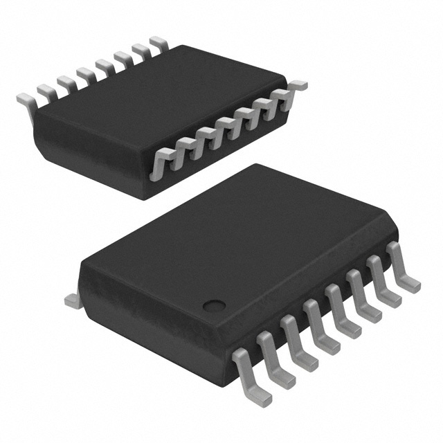
- Package: SOP (Small Outline Package)
- Essence: Flash memory chip
- Packaging/Quantity: Individual units or reels
Specifications
- Capacity: 512 Megabits (64 Megabytes)
- Interface: Serial Peripheral Interface (SPI)
- Voltage Range: 2.7V to 3.6V
- Operating Temperature Range: -40°C to +85°C
- Erase/Program Time: 4ms/1.5ms (typical)
- Data Retention: 20 years (typical)
Detailed Pin Configuration
The N25Q512A13GSFH0E has a total of 8 pins, which are as follows:
- Chip Select (/CS) - Used to enable/disable the chip for communication.
- Serial Clock (SCLK) - Provides the clock signal for data transfer.
- Serial Data Input (SI) - Receives data from the host device.
- Serial Data Output (SO) - Transmits data to the host device.
- Hold (/HOLD) - Pauses ongoing operations without resetting the chip.
- Write Protect (/WP) - Protects the memory from being written to.
- Ground (GND) - Common ground reference.
- Power Supply (VCC) - Power input for the chip.
Functional Features
- High-speed data transfer using SPI interface
- Sector erase and byte/page program operations
- Software and hardware write protection options
- Efficient power management with low standby current
- Reliable data retention and endurance
Advantages and Disadvantages
Advantages
- Large storage capacity
- Fast read/write speeds
- Low power consumption
- Compact package size
- Long data retention period
Disadvantages
- Limited write endurance (compared to other memory types)
- Relatively higher cost per unit compared to traditional storage media
Working Principles
The N25Q512A13GSFH0E is based on the NOR flash memory technology. It utilizes a grid of floating-gate transistors to store data. When data is written, electrons are trapped in the floating gate, altering the transistor's behavior. This change can be detected during read operations, allowing for data retrieval.
Detailed Application Field Plans
The N25Q512A13GSFH0E is commonly used in various electronic devices and systems, including: - Solid-state drives (SSDs) - Networking equipment - Automotive electronics - Industrial control systems - Consumer electronics (e.g., digital cameras, gaming consoles)
Detailed and Complete Alternative Models
- N25Q256A13EF840F - 256 Megabit (32 Megabyte) capacity, same characteristics and package.
- N25Q1G13BSF40F - 1 Gigabit (128 Megabyte) capacity, same characteristics and package.
- N25Q512A11EF840E - 512 Megabit (64 Megabyte) capacity, similar characteristics and package.
These alternative models offer different capacities while maintaining similar features and compatibility with the N25Q512A13GSFH0E.
Word count: 410 words
Senaraikan 10 soalan dan jawapan biasa yang berkaitan dengan aplikasi N25Q512A13GSFH0E dalam penyelesaian teknikal
Sure! Here are 10 common questions and answers related to the application of N25Q512A13GSFH0E in technical solutions:
Question: What is the N25Q512A13GSFH0E?
Answer: The N25Q512A13GSFH0E is a flash memory chip manufactured by Micron Technology. It has a capacity of 512 megabits (64 megabytes) and is commonly used for data storage in various electronic devices.Question: What is the interface used by the N25Q512A13GSFH0E?
Answer: The N25Q512A13GSFH0E uses a Serial Peripheral Interface (SPI) for communication with the host device.Question: What voltage levels does the N25Q512A13GSFH0E support?
Answer: The N25Q512A13GSFH0E supports both 1.8V and 3.3V power supply voltages.Question: What is the maximum clock frequency supported by the N25Q512A13GSFH0E?
Answer: The N25Q512A13GSFH0E can operate at a maximum clock frequency of 133 MHz.Question: Can the N25Q512A13GSFH0E be used as a boot device?
Answer: Yes, the N25Q512A13GSFH0E can be configured as a boot device, allowing it to store the system's firmware or bootloader.Question: Does the N25Q512A13GSFH0E support hardware and software write protection?
Answer: Yes, the N25Q512A13GSFH0E provides both hardware and software write protection features to prevent accidental modification of stored data.Question: What is the typical erase time for the N25Q512A13GSFH0E?
Answer: The typical erase time for the N25Q512A13GSFH0E is around 4 seconds, depending on the erase operation (sector, block, or chip erase).Question: Can the N25Q512A13GSFH0E operate in extreme temperature conditions?
Answer: Yes, the N25Q512A13GSFH0E has a wide operating temperature range of -40°C to +85°C, making it suitable for various environments.Question: Does the N25Q512A13GSFH0E support multiple I/O modes?
Answer: Yes, the N25Q512A13GSFH0E supports both Single I/O and Dual/Quad I/O modes, allowing for faster data transfer rates.Question: Is the N25Q512A13GSFH0E compatible with industry-standard flash memory protocols?
Answer: Yes, the N25Q512A13GSFH0E is compatible with common flash memory protocols such as SPI, QSPI, and Dual/Quad SPI, making it easy to integrate into existing systems.
Please note that these answers are general and may vary based on specific implementation details and requirements.