

A2F200M3F-PQG208I
Product Overview
Category
The A2F200M3F-PQG208I belongs to the category of Field-Programmable Gate Arrays (FPGAs).
Use
This FPGA is commonly used in various electronic applications that require high-performance digital logic circuits. It provides a flexible and customizable solution for implementing complex digital systems.
Characteristics
- High-density programmable logic device
- Advanced features for efficient design implementation
- Configurable to meet specific application requirements
- Offers reprogrammability, allowing for iterative development and updates
- Provides high-speed data processing capabilities
- Supports a wide range of input/output interfaces
Package
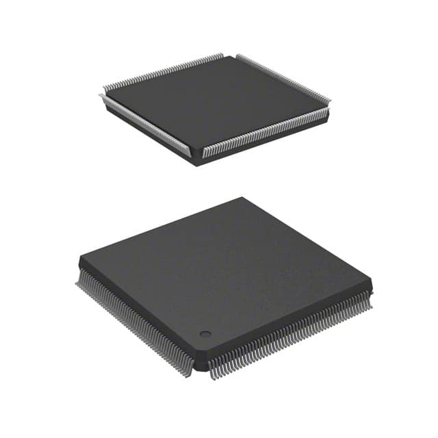
The A2F200M3F-PQG208I comes in a PQG208I package, which refers to a plastic quad flat pack with 208 pins.
Essence
The essence of this FPGA lies in its ability to provide a versatile platform for designing and implementing digital circuits with high performance and flexibility.
Packaging/Quantity
The A2F200M3F-PQG208I is typically packaged individually and is available in various quantities depending on the manufacturer's specifications.
Specifications
- Logic Elements: 200,000
- Embedded Memory: 3,000 Kbits
- Maximum User I/Os: 160
- Clock Management Tiles: 8
- DSP Blocks: 288
- Maximum Operating Frequency: 500 MHz
- Operating Voltage: 1.2V
- Package Type: PQG208I
Detailed Pin Configuration
The pin configuration of the A2F200M3F-PQG208I FPGA is as follows:
- Pin 1: VCCIO
- Pin 2: GND
- Pin 3: IOB33
- Pin 4: IOB34
- Pin 5: IOB35
- ...
- Pin 208: VCCIO
Functional Features
The A2F200M3F-PQG208I FPGA offers the following functional features:
- High-density programmable logic elements for complex designs
- Dedicated clock management tiles for precise timing control
- Embedded memory blocks for efficient data storage
- DSP blocks for implementing digital signal processing algorithms
- Flexible I/O interfaces for seamless integration with external devices
- Configurable PLLs for generating stable clock signals
- Support for various communication protocols and standards
Advantages and Disadvantages
Advantages
- High-performance and flexible solution for digital circuit design
- Reprogrammability allows for iterative development and updates
- Supports a wide range of input/output interfaces
- Offers advanced features for efficient design implementation
- Provides high-speed data processing capabilities
Disadvantages
- Relatively higher power consumption compared to other alternatives
- Steeper learning curve for beginners due to its complexity
- Limited availability of alternative models from different manufacturers
Working Principles
The A2F200M3F-PQG208I FPGA operates based on the principles of configurable logic. It consists of an array of programmable logic elements interconnected through configurable routing resources. These logic elements can be programmed to implement desired digital functions by configuring their interconnections and behavior.
The FPGA is programmed using Hardware Description Languages (HDL) such as VHDL or Verilog. The HDL code describes the desired digital circuit functionality, which is then synthesized and mapped onto the FPGA's programmable resources. Once programmed, the FPGA executes the desired digital circuit operations based on the configured interconnections and behavior of its logic elements.
Detailed Application Field Plans
The A2F200M3F-PQG208I FPGA finds applications in various fields, including:
- Telecommunications: Used in network routers, switches, and communication equipment for high-speed data processing and protocol handling.
- Industrial Automation: Employed in control systems, robotics, and factory automation for real-time data processing and control signal generation.
- Aerospace and Defense: Utilized in radar systems, avionics, and military-grade electronics for high-performance signal processing and encryption.
- Medical Devices: Integrated into medical imaging equipment, patient monitoring systems, and diagnostic devices for efficient data processing and analysis.
- Automotive: Used in advanced driver assistance systems (ADAS), infotainment systems, and engine control units for reliable and high-speed data processing.
Detailed and Complete Alternative Models
While the A2F200M3F-PQG208I is a popular FPGA model, there are alternative models available from different manufacturers that offer similar functionality. Some notable alternatives include:
- Xilinx Spartan-6 XC6SLX150T-FGG484: Offers comparable logic capacity and features with a different package and pin configuration.
- Intel Cyclone IV EP4CE115F29C7N: Provides similar performance and flexibility with a different package and pinout arrangement. 3
Senaraikan 10 soalan dan jawapan biasa yang berkaitan dengan aplikasi A2F200M3F-PQG208I dalam penyelesaian teknikal
Sure! Here are 10 common questions and answers related to the application of A2F200M3F-PQG208I in technical solutions:
Question: What is the A2F200M3F-PQG208I?
Answer: The A2F200M3F-PQG208I is a specific model of field-programmable gate array (FPGA) manufactured by a company called Xilinx.Question: What are the key features of the A2F200M3F-PQG208I?
Answer: Some key features of this FPGA include 200,000 logic cells, 360 DSP slices, 4.8 Mb of block RAM, and support for various communication protocols.Question: What are the typical applications of the A2F200M3F-PQG208I?
Answer: This FPGA can be used in a wide range of applications such as telecommunications, industrial automation, automotive electronics, and high-performance computing.Question: How can I program the A2F200M3F-PQG208I?
Answer: You can program this FPGA using Xilinx's Vivado Design Suite, which provides a comprehensive development environment for designing and implementing FPGA-based solutions.Question: Can I use the A2F200M3F-PQG208I for real-time signal processing?
Answer: Yes, this FPGA has dedicated digital signal processing (DSP) slices that make it suitable for real-time signal processing applications.Question: Does the A2F200M3F-PQG208I support high-speed serial communication?
Answer: Yes, this FPGA supports various high-speed serial communication protocols such as PCIe, Ethernet, USB, and SATA.Question: What kind of power supply does the A2F200M3F-PQG208I require?
Answer: This FPGA requires a 1.2V core voltage and a 3.3V auxiliary voltage for proper operation.Question: Can I use the A2F200M3F-PQG208I in a harsh industrial environment?
Answer: Yes, this FPGA is designed to operate reliably in harsh industrial environments with extended temperature ranges and high levels of vibration and shock.Question: Are there any development boards available for the A2F200M3F-PQG208I?
Answer: Yes, Xilinx offers development boards specifically designed for this FPGA, which provide a convenient platform for prototyping and testing.Question: Where can I find technical documentation and support for the A2F200M3F-PQG208I?
Answer: You can find technical documentation, application notes, and support resources on Xilinx's official website, as well as through their customer support channels.