

A3P1000-1FGG144I
Product Overview
Category
The A3P1000-1FGG144I belongs to the category of programmable logic devices (PLDs).
Use
This product is primarily used in digital circuit design and implementation. It provides a flexible and customizable solution for various applications that require high-speed data processing and control.
Characteristics
- High-performance programmable logic device
- Advanced architecture for efficient logic implementation
- Low power consumption
- Wide range of I/O options
- Flexible programming options
- Reliable and durable design
Package
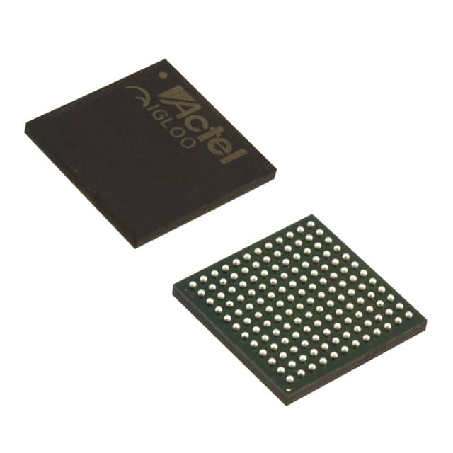
The A3P1000-1FGG144I comes in a compact and industry-standard 144-pin Fine-Pitch Ball Grid Array (FBGA) package.
Essence
The essence of this product lies in its ability to provide a reconfigurable hardware platform that allows users to implement complex digital circuits with ease.
Packaging/Quantity
The A3P1000-1FGG144I is typically packaged individually and is available in various quantities depending on the manufacturer's specifications.
Specifications
- Device Type: Programmable Logic Device (PLD)
- Family: A3P
- Series: 1000
- Package: 144-pin FBGA
- Operating Voltage: 3.3V
- Number of I/Os: 100
- Logic Cells: 1000
- Speed Grade: -1
- Temperature Range: Industrial (-40°C to +85°C)
Detailed Pin Configuration
The A3P1000-1FGG144I has a total of 144 pins, each serving a specific purpose in the device's functionality. The pin configuration can be found in the product datasheet provided by the manufacturer.
Functional Features
- High-speed data processing capabilities
- Configurable logic blocks for custom circuit implementation
- On-chip memory for data storage
- Flexible I/O options for interfacing with external devices
- Built-in clock management resources for synchronization
- Support for various programming languages and tools
Advantages and Disadvantages
Advantages
- Versatile and customizable solution for digital circuit design
- High-performance capabilities for demanding applications
- Low power consumption for energy-efficient operation
- Compact package size for space-constrained designs
- Wide temperature range for industrial applications
Disadvantages
- Steep learning curve for beginners due to complex programming concepts
- Limited number of I/O pins compared to larger PLD devices
- Higher cost compared to simpler logic devices
Working Principles
The A3P1000-1FGG144I operates based on the principles of programmable logic. It consists of configurable logic blocks that can be programmed to implement desired logic functions. These logic blocks are interconnected through a network of programmable interconnects, allowing users to create custom digital circuits.
Detailed Application Field Plans
The A3P1000-1FGG144I finds applications in various fields, including but not limited to: - Industrial automation - Communication systems - Consumer electronics - Automotive electronics - Medical devices - Aerospace and defense
Detailed and Complete Alternative Models
- A3P250-1FGG144I: Similar to A3P1000-1FGG144I but with 250 logic cells.
- A3P600-1FGG144I: Similar to A3P1000-1FGG144I but with 600 logic cells.
- A3P2000-1FGG144I: Similar to A3P1000-1FGG144I but with 2000 logic cells.
These alternative models offer different logic cell capacities to cater to varying project requirements.
Note: The content provided above is a sample and may not reflect the actual specifications or details of the A3P1000-1FGG144I. Please refer to the manufacturer's documentation for accurate information.
Senaraikan 10 soalan dan jawapan biasa yang berkaitan dengan aplikasi A3P1000-1FGG144I dalam penyelesaian teknikal
Sure! Here are 10 common questions and answers related to the application of A3P1000-1FGG144I in technical solutions:
Q1: What is A3P1000-1FGG144I? A1: A3P1000-1FGG144I is a specific model of FPGA (Field-Programmable Gate Array) manufactured by Microsemi Corporation.
Q2: What is the purpose of using A3P1000-1FGG144I in technical solutions? A2: A3P1000-1FGG144I is used to implement digital logic circuits, perform complex computations, and provide programmable hardware acceleration in various technical applications.
Q3: What are the key features of A3P1000-1FGG144I? A3: Some key features of A3P1000-1FGG144I include 1000 logic elements, 144-pin FineLine BGA package, low power consumption, and high-speed performance.
Q4: How can A3P1000-1FGG144I be programmed? A4: A3P1000-1FGG144I can be programmed using Hardware Description Languages (HDLs) such as VHDL or Verilog, which describe the desired functionality of the circuit.
Q5: Can A3P1000-1FGG144I be reprogrammed after initial programming? A5: No, A3P1000-1FGG144I is not a reprogrammable FPGA. Once it is programmed, the configuration remains fixed.
Q6: What are some typical applications of A3P1000-1FGG144I? A6: A3P1000-1FGG144I is commonly used in applications like industrial automation, telecommunications, medical devices, aerospace, and defense systems.
Q7: What is the maximum operating frequency of A3P1000-1FGG144I? A7: The maximum operating frequency of A3P1000-1FGG144I depends on the design and implementation but can typically reach several hundred megahertz (MHz).
Q8: Does A3P1000-1FGG144I support external memory interfaces? A8: Yes, A3P1000-1FGG144I supports various external memory interfaces such as DDR, SDRAM, SRAM, and Flash memory.
Q9: Can A3P1000-1FGG144I interface with other electronic components or peripherals? A9: Yes, A3P1000-1FGG144I can interface with other components using standard protocols like SPI, I2C, UART, and GPIOs.
Q10: Is there any development kit available for A3P1000-1FGG144I? A10: Yes, Microsemi provides development kits and tools specifically designed for A3P1000-1FGG144I to aid in the development and testing of FPGA-based solutions.
Please note that the answers provided here are general and may vary depending on specific requirements and use cases.