

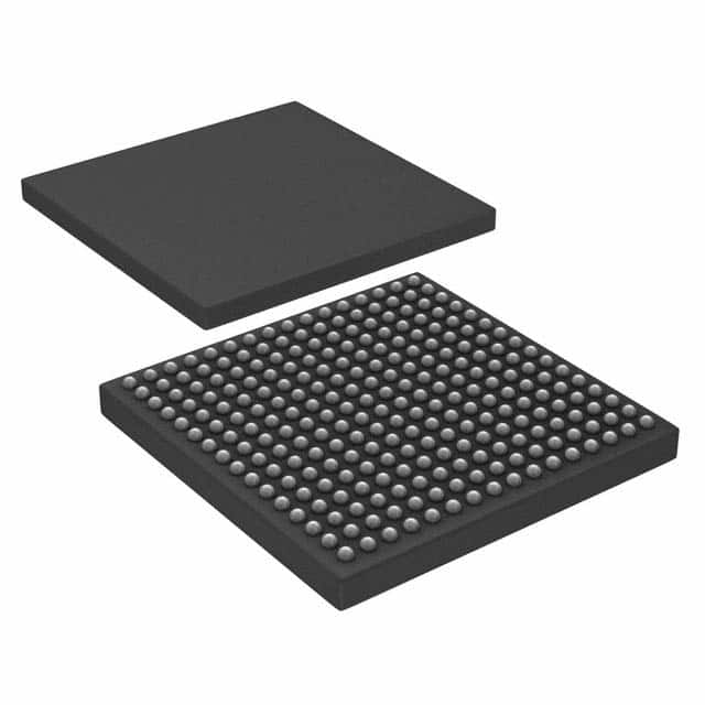
M2S010-VFG256I
Product Overview
Category
M2S010-VFG256I belongs to the category of programmable logic devices (PLDs).
Use
This product is used for implementing digital logic circuits and systems in various electronic applications.
Characteristics
- Programmable: The M2S010-VFG256I can be configured to perform specific functions based on user requirements.
- Versatile: It supports a wide range of applications due to its flexible programming capabilities.
- High-performance: The device offers fast processing speeds and efficient resource utilization.
- Low power consumption: It is designed to minimize power usage, making it suitable for battery-powered devices.
Package
The M2S010-VFG256I comes in a VFG256I package.
Essence
The essence of this product lies in its ability to provide a reconfigurable hardware platform that enables the implementation of complex digital designs.
Packaging/Quantity
Each package contains one M2S010-VFG256I device.
Specifications
- Logic Elements: 10,000
- Flip-Flops: 5,120
- Block RAM: 288 Kbits
- Maximum User I/Os: 202
- Operating Voltage: 1.2V
- Speed Grade: -6
Detailed Pin Configuration
The M2S010-VFG256I has a total of 256 pins. The pin configuration is as follows:
- Pin 1: GND
- Pin 2: IO0
- Pin 3: IO1
- ...
- Pin 255: IO253
- Pin 256: VCC
Functional Features
- Reconfigurability: The M2S010-VFG256I allows users to modify the functionality of the device by reprogramming it.
- Embedded Memory: It includes block RAM, which can be used for data storage and retrieval.
- I/O Flexibility: The device offers a large number of user I/Os, providing flexibility in connecting to external components.
- Clock Management: It supports various clocking options for synchronization and timing control.
Advantages and Disadvantages
Advantages
- Flexibility: The reconfigurable nature of the M2S010-VFG256I allows for quick prototyping and design iterations.
- Cost-effective: By using a single programmable device, multiple fixed-function chips can be replaced, reducing overall costs.
- Time-to-market: The ability to rapidly modify designs enables faster product development cycles.
Disadvantages
- Complexity: Programming and configuring the device may require specialized knowledge and tools.
- Limited Resources: Compared to dedicated ASICs or FPGAs, the M2S010-VFG256I has limited logic elements and memory capacity.
Working Principles
The M2S010-VFG256I is based on field-programmable gate array (FPGA) technology. It consists of configurable logic blocks interconnected through programmable routing resources. These logic blocks can be programmed to implement desired digital functions by configuring their internal look-up tables, flip-flops, and interconnections.
Detailed Application Field Plans
The M2S010-VFG256I finds applications in various fields, including:
- Embedded Systems: It can be used to implement control and communication interfaces in embedded systems.
- Communications: The device can be utilized for protocol conversion, signal processing, and encryption/decryption tasks.
- Industrial Automation: It enables the implementation of complex control algorithms and real-time monitoring systems.
- Automotive: The M2S010-VFG256I can be employed in automotive electronics for functions like engine management and driver assistance systems.
Detailed and Complete Alternative Models
- M2S050-VFG256I: A higher-capacity version with 50,000 logic elements and 8,192 flip-flops.
- M2S025-VFG256I: A lower-capacity version with 2,500 logic elements and 1,280 flip-flops.
- M2S005-VFG256I: A smaller variant with 500 logic elements and 256 flip-flops.
These alternative models provide options with varying capacities to suit different project requirements.
Word count: 550 words
Senaraikan 10 soalan dan jawapan biasa yang berkaitan dengan aplikasi M2S010-VFG256I dalam penyelesaian teknikal
Sure! Here are 10 common questions and answers related to the application of M2S010-VFG256I in technical solutions:
Q: What is M2S010-VFG256I? A: M2S010-VFG256I is a specific model of a field-programmable gate array (FPGA) manufactured by Microsemi.
Q: What are the key features of M2S010-VFG256I? A: Some key features include 10,000 logic elements, 256-pin FineLine BGA package, 3.3V operation, and support for various I/O standards.
Q: What are the typical applications of M2S010-VFG256I? A: M2S010-VFG256I can be used in a wide range of applications such as industrial automation, telecommunications, medical devices, and automotive systems.
Q: How does M2S010-VFG256I differ from other FPGAs? A: M2S010-VFG256I offers a balance between cost, performance, and power consumption, making it suitable for many mid-range applications.
Q: Can M2S010-VFG256I be programmed using industry-standard tools? A: Yes, M2S010-VFG256I can be programmed using popular FPGA development tools like Libero SoC Design Suite and Synplify Pro.
Q: What is the maximum clock frequency supported by M2S010-VFG256I? A: The maximum clock frequency depends on the design and implementation, but typically ranges from tens to hundreds of megahertz.
Q: Does M2S010-VFG256I support external memory interfaces? A: Yes, M2S010-VFG256I supports various memory interfaces such as DDR3, DDR2, and LPDDR.
Q: Can M2S010-VFG256I interface with other devices or protocols? A: Yes, M2S010-VFG256I supports a wide range of communication interfaces including UART, SPI, I2C, Ethernet, and USB.
Q: What is the power consumption of M2S010-VFG256I? A: The power consumption depends on the design and utilization of the FPGA, but typically ranges from a few hundred milliwatts to a few watts.
Q: Are there any development boards available for M2S010-VFG256I? A: Yes, Microsemi offers development boards specifically designed for M2S010-VFG256I, which provide a platform for prototyping and evaluation.
Please note that the answers provided here are general and may vary depending on specific requirements and use cases.