

M2S050S-1FG896I
Product Overview
Category
The M2S050S-1FG896I belongs to the category of Field Programmable Gate Arrays (FPGAs).
Use
FPGAs are integrated circuits that can be programmed and reprogrammed to perform various digital functions. The M2S050S-1FG896I is specifically designed for applications requiring high-performance and flexibility.
Characteristics
- High-performance FPGA with advanced features
- Flexible and reprogrammable design
- Suitable for a wide range of applications
- Compact package for easy integration
Package
The M2S050S-1FG896I comes in a compact and durable package, ensuring protection during handling and installation.
Essence
The essence of the M2S050S-1FG896I lies in its ability to provide a versatile and customizable solution for digital circuit implementation.
Packaging/Quantity
The M2S050S-1FG896I is typically packaged individually and is available in various quantities depending on customer requirements.
Specifications
- Model: M2S050S-1FG896I
- Family: M2S
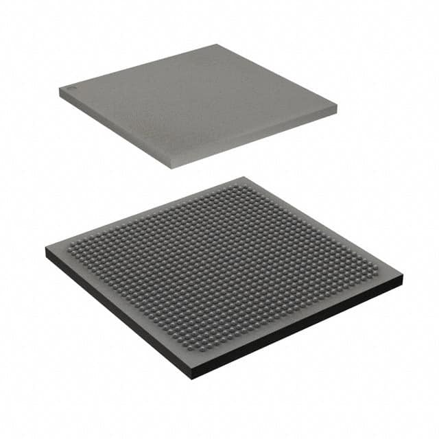
- Package: 896-pin Fine-Pitch Ball Grid Array (FBGA)
- Logic Cells: 50,000
- Embedded Memory: Up to 4.5 Mb
- Maximum User I/Os: 500
- Operating Voltage: 1.2V
- Speed Grade: -1
- Temperature Range: -40°C to +100°C
Detailed Pin Configuration
The M2S050S-1FG896I has a total of 896 pins arranged in a Fine-Pitch Ball Grid Array (FBGA) package. The pin configuration includes dedicated input/output pins, power supply pins, ground pins, and configuration pins. A detailed pinout diagram can be found in the product datasheet.
Functional Features
- High-performance FPGA architecture
- Configurable logic blocks for flexible circuit implementation
- Dedicated DSP blocks for efficient signal processing
- Embedded memory blocks for data storage
- Flexible I/O interfaces for easy integration with external devices
- Clock management resources for precise timing control
- Built-in configuration interface for easy programming
Advantages and Disadvantages
Advantages
- Versatile and customizable solution for digital circuit implementation
- High-performance capabilities for demanding applications
- Reprogrammable design allows for iterative development and updates
- Compact package enables easy integration into various systems
Disadvantages
- Requires expertise in FPGA programming for optimal utilization
- Higher cost compared to fixed-function integrated circuits
- Limited availability of alternative models with similar specifications
Working Principles
The M2S050S-1FG896I operates based on the principles of field-programmable gate arrays. It consists of configurable logic blocks, embedded memory, I/O interfaces, and other resources that can be programmed using hardware description languages (HDLs) such as VHDL or Verilog. The user designs a digital circuit by specifying the desired functionality and interconnections within the FPGA. The design is then synthesized, implemented, and loaded onto the M2S050S-1FG896I, allowing it to perform the specified functions.
Detailed Application Field Plans
The M2S050S-1FG896I finds applications in various fields, including but not limited to: - Telecommunications - Industrial automation - Aerospace and defense - Medical devices - Automotive electronics - Consumer electronics
In telecommunications, the M2S050S-1FG896I can be used for high-speed data processing, protocol conversion, and network packet routing. In industrial automation, it can enable real-time control systems, motor control, and sensor interfacing. In aerospace and defense, it can be utilized for radar signal processing, encryption, and secure communication. In medical devices, it can assist in image processing, patient monitoring, and diagnostics. In automotive electronics, it can contribute to advanced driver assistance systems (ADAS), infotainment, and engine control. In consumer electronics, it can support video and audio processing, gaming, and multimedia applications.
Detailed and Complete Alternative Models
While the M2S050S-1FG896I offers a unique combination of features and specifications, there are alternative models available from other FPGA manufacturers that may suit specific requirements. Some notable alternatives include: - Xilinx Spartan-6 XC6SLX150 - Intel Cyclone IV EP4CE115 - Lattice ECP5-85 - Microsemi SmartFusion2 M2S010S
These alternative models offer varying capabilities, package options, and price points, providing customers with a range of choices based on their specific needs.
In conclusion, the M2S050S-1FG896I is a high-performance FPGA that offers flexibility, versatility, and advanced features. Its compact design, extensive pin
Senaraikan 10 soalan dan jawapan biasa yang berkaitan dengan aplikasi M2S050S-1FG896I dalam penyelesaian teknikal
Sure! Here are 10 common questions and answers related to the application of M2S050S-1FG896I in technical solutions:
Q1: What is M2S050S-1FG896I? A1: M2S050S-1FG896I is a specific model of field-programmable gate array (FPGA) manufactured by Microsemi. It is designed for various technical applications.
Q2: What are the key features of M2S050S-1FG896I? A2: Some key features of M2S050S-1FG896I include 50,000 logic elements, 1.2V core voltage, 896-pin FineLine BGA package, and support for various I/O standards.
Q3: What are the typical applications of M2S050S-1FG896I? A3: M2S050S-1FG896I can be used in a wide range of applications such as industrial automation, telecommunications, automotive electronics, medical devices, and more.
Q4: How can M2S050S-1FG896I be programmed? A4: M2S050S-1FG896I can be programmed using industry-standard hardware description languages (HDLs) like VHDL or Verilog. Programming tools provided by Microsemi can be used for synthesis, simulation, and programming.
Q5: What are the power requirements for M2S050S-1FG896I? A5: M2S050S-1FG896I operates at a core voltage of 1.2V. The power requirements may vary depending on the specific application and configuration.
Q6: Can M2S050S-1FG896I interface with other components or devices? A6: Yes, M2S050S-1FG896I supports various I/O standards and can interface with other components or devices such as sensors, memory modules, communication interfaces, and more.
Q7: Is M2S050S-1FG896I suitable for high-speed applications? A7: Yes, M2S050S-1FG896I is designed to handle high-speed applications. It offers features like high-performance logic fabric, dedicated clock management resources, and support for high-speed I/O standards.
Q8: Can M2S050S-1FG896I be reprogrammed after deployment? A8: Yes, M2S050S-1FG896I is a field-programmable device, which means it can be reprogrammed even after deployment. This allows for flexibility and adaptability in the system design.
Q9: Are there any development kits available for M2S050S-1FG896I? A9: Yes, Microsemi provides development kits specifically designed for M2S050S-1FG896I. These kits include necessary hardware, software tools, documentation, and example designs to aid in the development process.
Q10: Where can I find technical support or documentation for M2S050S-1FG896I? A10: Microsemi provides technical support through their website, where you can find documentation, application notes, user guides, and contact information for further assistance.
Please note that the specific details and answers may vary depending on the manufacturer's documentation and specifications.