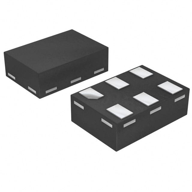
74AUP1G07GM,132
Basic Information Overview
- Category: Integrated Circuit (IC)
- Use: Logic Gate Buffer/Driver
- Characteristics: Single Buffer with Open Drain Output
- Package: SOT353 (SC-88A)
- Essence: Low-power, high-speed CMOS technology
- Packaging/Quantity: Tape and Reel, 3000 pieces per reel
Specifications
- Supply Voltage Range: 0.8V to 3.6V
- Input Voltage Range: -0.5V to VCC + 0.5V
- Output Voltage Range: 0V to VCC
- Maximum Operating Frequency: 2.5GHz
- Propagation Delay: 1.9ns (typical)
- Output Drive Capability: 32mA (maximum)
Detailed Pin Configuration
The 74AUP1G07GM,132 IC has the following pin configuration: - Pin 1: GND (Ground) - Pin 2: Input - Pin 3: Output
Functional Features
- Single buffer with open drain output
- Compatible with various logic families
- High-speed operation
- Low power consumption
- Wide supply voltage range
- ESD protection for robustness
Advantages and Disadvantages
Advantages: - Low power consumption makes it suitable for battery-powered devices - High-speed operation allows for quick signal processing - Wide supply voltage range enables compatibility with different systems - ESD protection ensures reliability in harsh environments
Disadvantages: - Limited output drive capability may not be suitable for high-current applications - Only one buffer available per IC, limiting the number of outputs
Working Principles
The 74AUP1G07GM,132 is a logic gate buffer/driver that amplifies and shapes digital signals. It operates using low-power, high-speed CMOS technology. The input signal is buffered and then provided as an open drain output. The IC can be powered by a supply voltage ranging from 0.8V to 3.6V, making it compatible with various systems.
Detailed Application Field Plans
The 74AUP1G07GM,132 IC finds applications in various fields, including: - Consumer electronics: smartphones, tablets, portable media players - Automotive: infotainment systems, lighting controls - Industrial automation: sensor interfaces, motor control - Communication systems: routers, switches, network equipment
Detailed and Complete Alternative Models
Some alternative models that offer similar functionality to the 74AUP1G07GM,132 IC include: - SN74LVC1G07DBVR (Texas Instruments) - MC74VHC1GT07DF1G (ON Semiconductor) - NC7SZ07P5X (Fairchild Semiconductor)
(Note: The above list is not exhaustive and there may be other alternative models available in the market.)
This entry provides an overview of the 74AUP1G07GM,132 IC, including its basic information, specifications, pin configuration, functional features, advantages and disadvantages, working principles, application field plans, and alternative models. It serves as a comprehensive reference for users seeking information about this logic gate buffer/driver IC.
Senaraikan 10 soalan dan jawapan biasa yang berkaitan dengan aplikasi 74AUP1G07GM,132 dalam penyelesaian teknikal
Sure! Here are 10 common questions and answers related to the application of 74AUP1G07GM,132 in technical solutions:
Q1: What is the function of the 74AUP1G07GM,132? A1: The 74AUP1G07GM,132 is a single buffer/driver with open-drain output. It can be used for level shifting, signal buffering, and driving low-power devices.
Q2: What is the operating voltage range of the 74AUP1G07GM,132? A2: The 74AUP1G07GM,132 operates within a voltage range of 0.8V to 3.6V.
Q3: What is the maximum output current of the 74AUP1G07GM,132? A3: The maximum output current of the 74AUP1G07GM,132 is typically 32mA.
Q4: Can the 74AUP1G07GM,132 be used for bidirectional communication? A4: No, the 74AUP1G07GM,132 is a unidirectional buffer/driver and does not support bidirectional communication.
Q5: What is the typical propagation delay of the 74AUP1G07GM,132? A5: The typical propagation delay of the 74AUP1G07GM,132 is around 2.5ns.
Q6: Can the 74AUP1G07GM,132 be used in high-speed applications? A6: Yes, the 74AUP1G07GM,132 is designed for high-speed operation and can be used in applications with fast switching requirements.
Q7: Does the 74AUP1G07GM,132 have built-in ESD protection? A7: Yes, the 74AUP1G07GM,132 has built-in ESD protection, which helps to safeguard against electrostatic discharge.
Q8: Can the 74AUP1G07GM,132 drive capacitive loads? A8: Yes, the 74AUP1G07GM,132 can drive small capacitive loads. However, for larger capacitive loads, additional buffering may be required.
Q9: Is the 74AUP1G07GM,132 suitable for battery-powered applications? A9: Yes, the 74AUP1G07GM,132 is suitable for battery-powered applications as it operates within a low voltage range and has low power consumption.
Q10: What package options are available for the 74AUP1G07GM,132? A10: The 74AUP1G07GM,132 is available in various package options, including SOT353 and XSON6.


