

Lihat spesifikasi untuk butiran produk.
74HC1G125GV-Q100H
Product Overview
Category
The 74HC1G125GV-Q100H belongs to the category of integrated circuits (ICs).
Use
This IC is commonly used for signal buffering and level shifting in various electronic devices.
Characteristics
- High-speed operation
- Low power consumption
- Wide operating voltage range
- Schmitt-trigger action on all inputs
- Balanced propagation delays
- Symmetrical output impedance
- Overvoltage tolerant inputs
- ESD protection
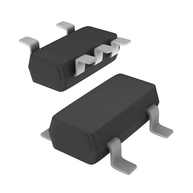
Package
The 74HC1G125GV-Q100H is available in a small SOT353 package, which is suitable for space-constrained applications.
Essence
The essence of this IC lies in its ability to provide reliable signal buffering and level shifting capabilities, ensuring proper signal integrity in electronic systems.
Packaging/Quantity
The 74HC1G125GV-Q100H is typically packaged in reels or tubes, with a quantity of 3000 units per reel/tube.
Specifications
- Supply voltage: 2.0V to 6.0V
- Input voltage: -0.5V to VCC + 0.5V
- Output voltage: -0.5V to VCC + 0.5V
- Operating temperature range: -40°C to +125°C
- Maximum static current: 8mA
- Maximum dynamic current: 20mA
Detailed Pin Configuration
The 74HC1G125GV-Q100H has a total of 5 pins:
- GND (Ground)
- OE (Output Enable)
- A (Input)
- Y (Output)
- VCC (Supply Voltage)
Functional Features
- The OE pin allows for enabling or disabling the output.
- The Schmitt-trigger action on all inputs ensures noise immunity and hysteresis.
- The balanced propagation delays ensure accurate signal transmission.
- The symmetrical output impedance facilitates matching with different loads.
- The overvoltage tolerant inputs protect the IC from voltage spikes.
- The ESD protection guards against electrostatic discharge.
Advantages and Disadvantages
Advantages
- High-speed operation enables efficient signal processing.
- Low power consumption prolongs battery life in portable devices.
- Wide operating voltage range allows compatibility with various systems.
- Schmitt-trigger action enhances noise immunity.
- Balanced propagation delays ensure accurate timing.
Disadvantages
- Limited number of input/output pins restricts the complexity of circuits that can be built solely using this IC.
- SOT353 package may require specialized handling during assembly.
Working Principles
The 74HC1G125GV-Q100H operates based on CMOS (Complementary Metal-Oxide-Semiconductor) technology. It utilizes a combination of MOSFET transistors to buffer and shift input signals, ensuring proper voltage levels and signal integrity throughout the circuit.
Detailed Application Field Plans
The 74HC1G125GV-Q100H finds applications in various electronic systems, including but not limited to: - Mobile devices - Consumer electronics - Industrial automation - Automotive electronics - Communication systems
Detailed and Complete Alternative Models
Some alternative models that offer similar functionality to the 74HC1G125GV-Q100H include: - SN74LVC1G125DBVR - MC74VHC1GT125DTT1G - TC7SZ125FU
These alternatives can be considered based on specific requirements, availability, and cost considerations.
Word count: 446 words
Senaraikan 10 soalan dan jawapan biasa yang berkaitan dengan aplikasi 74HC1G125GV-Q100H dalam penyelesaian teknikal
Sure! Here are 10 common questions and answers related to the application of 74HC1G125GV-Q100H in technical solutions:
Q1: What is the 74HC1G125GV-Q100H? A1: The 74HC1G125GV-Q100H is a single bus buffer gate with 3-state output, designed for use in various digital logic applications.
Q2: What is the voltage supply range for the 74HC1G125GV-Q100H? A2: The voltage supply range for this device is typically between 2.0V and 6.0V.
Q3: What is the maximum output current of the 74HC1G125GV-Q100H? A3: The maximum output current is 8mA.
Q4: Can the 74HC1G125GV-Q100H be used as a level shifter? A4: Yes, it can be used as a level shifter to convert signals between different voltage levels.
Q5: What is the operating temperature range for the 74HC1G125GV-Q100H? A5: The operating temperature range is typically between -40°C and 125°C.
Q6: How many inputs does the 74HC1G125GV-Q100H have? A6: It has one input.
Q7: How many outputs does the 74HC1G125GV-Q100H have? A7: It has one output.
Q8: Can the 74HC1G125GV-Q100H be used in high-speed applications? A8: Yes, it is suitable for high-speed applications with a maximum propagation delay of 9 ns.
Q9: Is the 74HC1G125GV-Q100H compatible with other logic families? A9: Yes, it is compatible with both CMOS and TTL logic families.
Q10: What is the package type for the 74HC1G125GV-Q100H? A10: It is available in a SOT753 package.
Please note that these answers are general and may vary depending on the specific datasheet and manufacturer's specifications.