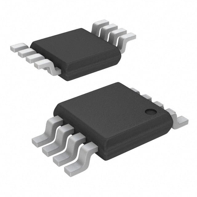
74HC3G34DP-Q100H
Basic Information Overview
- Category: Integrated Circuit (IC)
- Use: Logic Gate
- Characteristics: Triple Buffer/Inverter with Open Drain Outputs
- Package: TSSOP-8
- Essence: High-Speed CMOS Technology
- Packaging/Quantity: Tape and Reel, 2500 pieces per reel
Specifications
- Supply Voltage Range: 2.0V to 6.0V
- Input Voltage Range: -0.5V to VCC + 0.5V
- Output Voltage Range: -0.5V to VCC + 0.5V
- Maximum Operating Frequency: 140 MHz
- Propagation Delay: 4.5 ns (typical)
- Input Capacitance: 3 pF (typical)
- Output Capacitance: 6 pF (typical)
Detailed Pin Configuration
The 74HC3G34DP-Q100H has a TSSOP-8 package with the following pin configuration:
__    __
   Y1 |1  \/  8| VCC
   Y2 |2      7| A
   Y3 |3      6| B
 GND  |4      5| C
       ----------
Functional Features
- Triple buffer/inverter with open drain outputs
- High-speed operation
- Wide supply voltage range
- Low power consumption
- Schmitt-trigger action on all inputs
- Balanced propagation delays
- Overvoltage tolerant inputs
- Complies with JEDEC standard JESD8-7A
Advantages and Disadvantages
Advantages: - High-speed operation allows for efficient data processing. - Wide supply voltage range enables compatibility with various systems. - Low power consumption reduces energy usage. - Schmitt-trigger action ensures noise immunity. - Overvoltage tolerant inputs protect the IC from voltage spikes.
Disadvantages: - Limited number of buffer/inverter gates (3 in this case). - Open drain outputs may require additional pull-up resistors for certain applications.
Working Principles
The 74HC3G34DP-Q100H is a triple buffer/inverter IC that operates using high-speed CMOS technology. It consists of three independent buffer/inverter gates with open drain outputs. The inputs are equipped with Schmitt-trigger action, providing noise immunity and allowing for reliable signal processing. The IC operates within a wide supply voltage range and consumes low power, making it suitable for various applications.
Detailed Application Field Plans
The 74HC3G34DP-Q100H can be used in a wide range of applications, including but not limited to: 1. Digital communication systems 2. Microcontrollers and microprocessors 3. Data storage devices 4. Industrial automation 5. Automotive electronics 6. Consumer electronics
Detailed and Complete Alternative Models
- SN74LVC3G34-Q1: Triple Buffer/Inverter with Open Drain Outputs, VCC Range: 1.65V to 5.5V, Package: SOT-23-8
- MC74LCX125: Quad Buffer/Line Driver with 3-State Outputs, VCC Range: 2.0V to 3.6V, Package: SOIC-14
- CD74HC4049: Hex Inverting Buffer/Converter, VCC Range: 2.0V to 6.0V, Package: DIP-16
These alternative models offer similar functionality and can be considered as substitutes for the 74HC3G34DP-Q100H depending on specific requirements and design constraints.
Word count: 389 words
Senaraikan 10 soalan dan jawapan biasa yang berkaitan dengan aplikasi 74HC3G34DP-Q100H dalam penyelesaian teknikal
Sure! Here are 10 common questions and answers related to the application of 74HC3G34DP-Q100H in technical solutions:
Q: What is the 74HC3G34DP-Q100H? A: The 74HC3G34DP-Q100H is a triple buffer gate IC (Integrated Circuit) that can be used for signal buffering and level shifting applications.
Q: What is the operating voltage range of the 74HC3G34DP-Q100H? A: The operating voltage range of the 74HC3G34DP-Q100H is typically between 2V and 6V.
Q: How many buffer gates are there in the 74HC3G34DP-Q100H? A: The 74HC3G34DP-Q100H consists of three independent buffer gates.
Q: What is the maximum output current of each buffer gate in the 74HC3G34DP-Q100H? A: The maximum output current of each buffer gate in the 74HC3G34DP-Q100H is typically around 8mA.
Q: Can the 74HC3G34DP-Q100H be used for level shifting between different voltage domains? A: Yes, the 74HC3G34DP-Q100H can be used for level shifting between different voltage domains as long as the voltage levels are within its operating range.
Q: What is the propagation delay of the 74HC3G34DP-Q100H? A: The propagation delay of the 74HC3G34DP-Q100H is typically around 7 ns.
Q: Is the 74HC3G34DP-Q100H compatible with both CMOS and TTL logic levels? A: Yes, the 74HC3G34DP-Q100H is compatible with both CMOS and TTL logic levels.
Q: Can the 74HC3G34DP-Q100H be used for bidirectional signal buffering? A: No, the 74HC3G34DP-Q100H is a unidirectional buffer and cannot be used for bidirectional signal buffering.
Q: What is the package type of the 74HC3G34DP-Q100H? A: The 74HC3G34DP-Q100H is available in a TSSOP-8 package.
Q: Is the 74HC3G34DP-Q100H suitable for automotive applications? A: Yes, the 74HC3G34DP-Q100H is designed to meet the requirements of automotive applications and is qualified according to the AEC-Q100 standard.
Please note that the answers provided here are general and may vary depending on the specific datasheet and manufacturer's specifications of the 74HC3G34DP-Q100H.


