

74HCT238BQ,115
Product Overview
Category
The 74HCT238BQ,115 belongs to the category of integrated circuits (ICs).
Use
This IC is commonly used in digital electronics for decoding and demultiplexing applications.
Characteristics
- High-speed operation
- Low power consumption
- Wide operating voltage range
- Compatibility with TTL inputs
- Schmitt-trigger action on all inputs
- Balanced propagation delays
Package
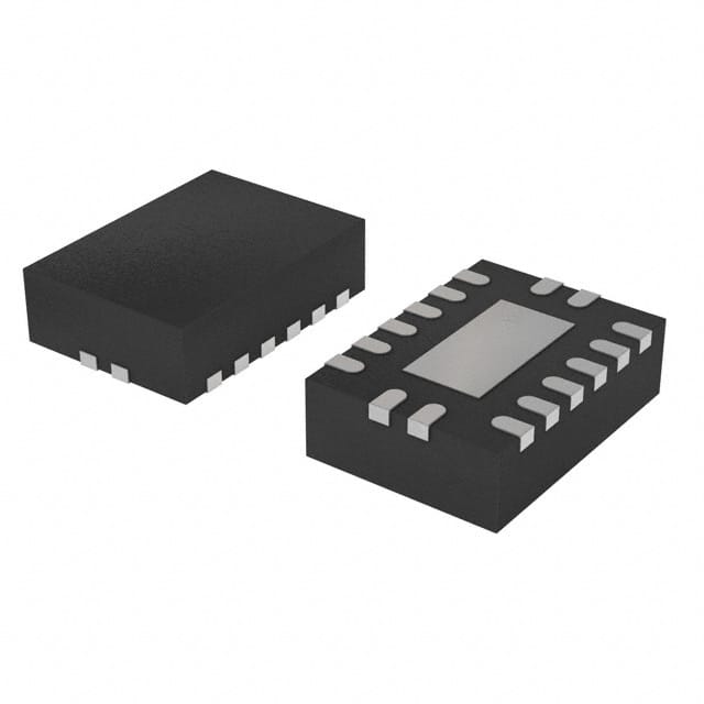
The 74HCT238BQ,115 is available in a small outline package (SOIC) with 16 pins.
Essence
The essence of this product lies in its ability to decode binary-coded inputs and select one of eight outputs based on the input combination.
Packaging/Quantity
The 74HCT238BQ,115 is typically packaged in reels or tubes, containing a specific quantity of ICs per package. The exact quantity may vary depending on the manufacturer's specifications.
Specifications
- Supply Voltage: 2.0V to 6.0V
- Input Voltage: -0.5V to VCC + 0.5V
- Output Voltage: -0.5V to VCC + 0.5V
- Operating Temperature Range: -40°C to +125°C
- Maximum Propagation Delay: 25 ns
Detailed Pin Configuration
The 74HCT238BQ,115 has 16 pins, which are labeled as follows:
- A0 (Input)
- A1 (Input)
- A2 (Input)
- GND (Ground)
- Y0 (Output)
- Y1 (Output)
- Y2 (Output)
- Y3 (Output)
- Y4 (Output)
- Y5 (Output)
- Y6 (Output)
- Y7 (Output)
- VCC (Power Supply)
- OE (Output Enable)
- GND (Ground)
- A3 (Input)
Functional Features
The 74HCT238BQ,115 offers the following functional features:
- Decodes three binary-coded inputs (A0, A1, A2) into eight mutually exclusive outputs (Y0-Y7).
- Output enable (OE) pin allows for disabling all outputs when necessary.
- Schmitt-trigger action on all inputs ensures noise immunity and improved signal integrity.
- Wide operating voltage range makes it compatible with various digital systems.
Advantages and Disadvantages
Advantages
- High-speed operation enables efficient decoding in time-critical applications.
- Low power consumption helps conserve energy in battery-powered devices.
- Compatibility with TTL inputs allows for easy integration with existing digital circuits.
- Balanced propagation delays ensure accurate timing synchronization.
Disadvantages
- Limited number of input combinations due to three-bit decoding capability.
- May require additional ICs or circuitry for complex decoding requirements.
Working Principles
The 74HCT238BQ,115 operates based on the principle of combinational logic. It uses the binary-coded inputs (A0, A1, A2) to select one of the eight outputs (Y0-Y7). The output enable (OE) pin controls the activation of the outputs. When OE is low, the outputs are enabled, and when OE is high, the outputs are disabled.
Detailed Application Field Plans
The 74HCT238BQ,115 finds applications in various fields, including but not limited to:
- Address decoding in microcontrollers and microprocessors.
- Memory selection in digital storage systems.
- Data demultiplexing in communication systems.
- Control signal generation in industrial automation.
- Input/output expansion in embedded systems.
Detailed and Complete Alternative Models
Some alternative models that offer similar functionality to the 74HCT238BQ,115 include:
- 74LS138: A TTL-compatible decoder/demultiplexer IC.
- CD74HC238: A high-speed CMOS decoder/demultiplexer IC.
- SN74LVC138A: A low-voltage CMOS decoder/demultiplexer IC.
These alternative models can be considered based on specific requirements and compatibility with existing systems.
Word count: 570 words
Senaraikan 10 soalan dan jawapan biasa yang berkaitan dengan aplikasi 74HCT238BQ,115 dalam penyelesaian teknikal
Sure! Here are 10 common questions and answers related to the application of 74HCT238BQ,115 in technical solutions:
Question: What is the function of the 74HCT238BQ,115?
Answer: The 74HCT238BQ,115 is a 3-to-8 line decoder/demultiplexer IC that converts binary input signals into corresponding output lines.Question: What is the maximum operating voltage for the 74HCT238BQ,115?
Answer: The maximum operating voltage for this IC is 5.5V.Question: How many input lines does the 74HCT238BQ,115 have?
Answer: It has three input lines (A0, A1, and A2) which are used to select one of the eight output lines.Question: What is the purpose of the enable pin (E) on the 74HCT238BQ,115?
Answer: The enable pin is used to enable or disable the decoder/demultiplexer. When E is high, the outputs are active; when E is low, the outputs are disabled.Question: Can the 74HCT238BQ,115 be cascaded to increase the number of output lines?
Answer: Yes, multiple 74HCT238BQ,115 ICs can be cascaded together to increase the number of output lines.Question: What is the typical propagation delay of the 74HCT238BQ,115?
Answer: The typical propagation delay is around 12 ns.Question: Can the 74HCT238BQ,115 be used with both TTL and CMOS logic levels?
Answer: Yes, it is compatible with both TTL and CMOS logic levels.Question: What is the maximum output current of the 74HCT238BQ,115?
Answer: The maximum output current per pin is 4 mA.Question: Can the 74HCT238BQ,115 be used in high-frequency applications?
Answer: Yes, it can be used in high-frequency applications as it has a wide operating frequency range.Question: Are there any specific precautions to consider when using the 74HCT238BQ,115?
Answer: It is important to ensure that the power supply voltage does not exceed the specified maximum limit (5.5V) to prevent damage to the IC. Additionally, proper decoupling capacitors should be used for stable operation.
Please note that these answers are general and may vary depending on the specific application and requirements.