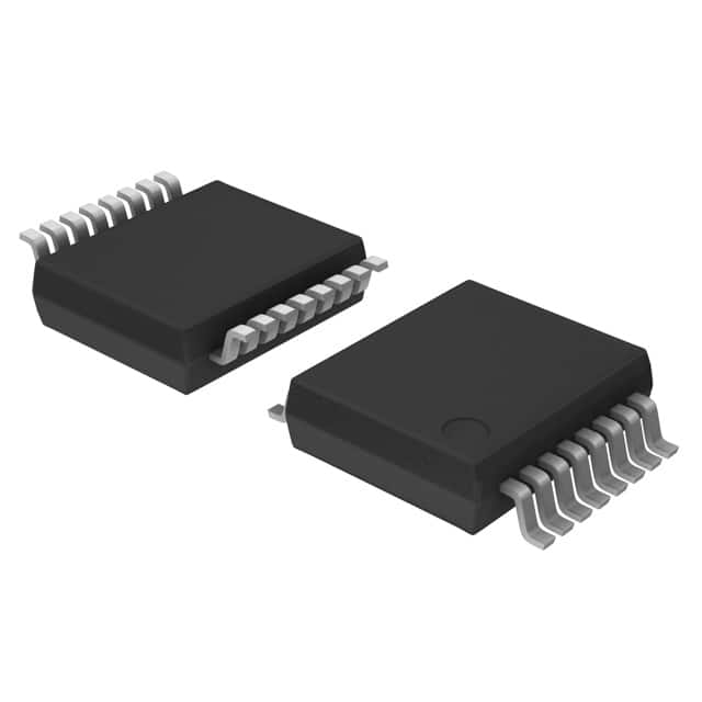
74HCT4094DB,112
Basic Information Overview
- Category: Integrated Circuit (IC)
- Use: Shift Register
- Characteristics: High-speed operation, low power consumption
- Package: SSOP-16
- Essence: Serial-in, parallel-out shift register with storage capability
- Packaging/Quantity: Tape and reel, 2500 units per reel
Specifications
- Supply Voltage: 2.0V to 6.0V
- Input Voltage: -0.5V to VCC + 0.5V
- Output Voltage: -0.5V to VCC + 0.5V
- Operating Temperature Range: -40°C to +125°C
- Maximum Clock Frequency: 100 MHz
Detailed Pin Configuration
- SER (Serial Data Input)
- RCLK (Register Clock Input)
- SRCLK (Shift Register Clock Input)
- OE (Output Enable Input)
- Q7' (Serial Output)
- GND (Ground)
- Q0-Q7 (Parallel Outputs)
- VCC (Supply Voltage)
Functional Features
- Serial-in, parallel-out shifting of data
- Storage capability for parallel outputs
- High-speed operation with a maximum clock frequency of 100 MHz
- Low power consumption
Advantages
- Allows efficient data transfer between microcontrollers and other digital devices
- Compact package size enables space-saving designs
- Wide operating voltage range allows compatibility with various systems
- High-speed operation facilitates quick data processing
Disadvantages
- Limited number of parallel outputs (8 in this case)
- Requires external clock signals for proper functioning
- Sensitive to voltage fluctuations, necessitating stable power supply
Working Principles
The 74HCT4094DB,112 is a serial-in, parallel-out shift register with storage capability. It receives data serially through the SER pin and shifts it into its internal register upon receiving a clock signal at the SRCLK pin. The RCLK pin is used to latch the parallel outputs (Q0-Q7) from the internal register. The OE pin enables or disables the output stage, allowing control over when the parallel outputs are active.
Detailed Application Field Plans
- Data storage and retrieval systems
- LED matrix displays
- Serial-to-parallel data conversion
- Digital communication interfaces
- Industrial automation control systems
Detailed and Complete Alternative Models
- 74HC4094: Similar functionality, but operates at a higher voltage range (2V to 6V)
- CD4094: Comparable shift register with storage capability, but operates at a lower clock frequency (up to 5 MHz)
- SN74HC595: Parallel-in, serial-out shift register with storage capability, suitable for different applications
(Note: These alternative models are just a few examples; there are several other options available in the market.)
This entry provides an overview of the 74HCT4094DB,112 integrated circuit, including its basic information, specifications, pin configuration, functional features, advantages, disadvantages, working principles, application field plans, and alternative models. With its high-speed operation, low power consumption, and compact package size, this shift register is widely used in various digital systems requiring efficient data transfer and storage capabilities.
Senaraikan 10 soalan dan jawapan biasa yang berkaitan dengan aplikasi 74HCT4094DB,112 dalam penyelesaian teknikal
Sure! Here are 10 common questions and answers related to the application of 74HCT4094DB,112 in technical solutions:
Q: What is the function of the 74HCT4094DB,112? A: The 74HCT4094DB,112 is an 8-bit serial-in/parallel-out shift register with output latches. It can be used for data storage, control signal generation, and driving LEDs or other digital devices.
Q: How does the 74HCT4094DB,112 work? A: The shift register receives data serially through a single input pin and shifts it internally. The shifted data can then be parallel-loaded into the output latches and simultaneously appear on the output pins.
Q: What is the maximum clock frequency supported by the 74HCT4094DB,112? A: The 74HCT4094DB,112 can operate at a maximum clock frequency of 25 MHz.
Q: Can the 74HCT4094DB,112 be cascaded to increase the number of outputs? A: Yes, multiple 74HCT4094DB,112 chips can be cascaded together to increase the number of outputs. The output of one chip can be connected to the input of the next chip.
Q: What is the power supply voltage range for the 74HCT4094DB,112? A: The 74HCT4094DB,112 operates with a power supply voltage range of 2 V to 6 V.
Q: Does the 74HCT4094DB,112 have built-in protection against electrostatic discharge (ESD)? A: Yes, the 74HCT4094DB,112 has ESD protection on all pins, making it more robust against ESD events.
Q: Can the 74HCT4094DB,112 be used with both CMOS and TTL logic levels? A: Yes, the 74HCT4094DB,112 is compatible with both CMOS and TTL logic levels, allowing it to interface with a wide range of digital systems.
Q: What is the typical output current capability of the 74HCT4094DB,112? A: The 74HCT4094DB,112 can typically source or sink up to 6 mA of current per output pin.
Q: Is the 74HCT4094DB,112 suitable for high-speed applications? A: Yes, the 74HCT4094DB,112 is designed for high-speed operation and can be used in applications that require fast data transfer.
Q: Are there any specific application notes or reference designs available for the 74HCT4094DB,112? A: Yes, the datasheet of the 74HCT4094DB,112 provides detailed application information, including timing diagrams and example circuits, which can be used as a reference for designing with this chip.
Please note that the specific part number mentioned (74HCT4094DB,112) may vary depending on the manufacturer or distributor.


