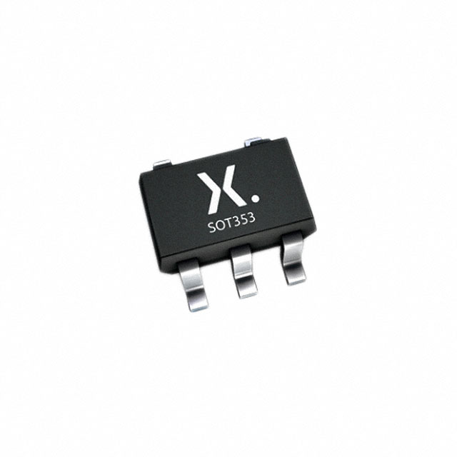
74LVC1G125GW-Q100
Basic Information Overview
- Category: Integrated Circuit (IC)
- Use: Buffer/Driver
- Characteristics: Low-voltage, single gate, non-inverting buffer/driver
- Package: SOT753 (SC-70)
- Essence: This IC is designed to provide a high-speed, low-power solution for buffering or driving signals in various electronic applications.
- Packaging/Quantity: Available in tape and reel packaging with 3000 units per reel.
Specifications
- Supply Voltage Range: 1.65V to 5.5V
- High-Level Input Voltage: 0.7 x VCC
- Low-Level Input Voltage: 0.3 x VCC
- Output Drive Capability: ±24mA
- Propagation Delay: 4.3ns (typical)
- Operating Temperature Range: -40°C to +125°C
Detailed Pin Configuration
The 74LVC1G125GW-Q100 IC has the following pin configuration:
____
   Y1 |    | VCC
   A  |    | Y2
 GND  |____| OE
Functional Features
- Non-inverting buffer/driver: The IC provides a non-inverted output signal compared to the input signal.
- Wide supply voltage range: It can operate within a wide range of supply voltages from 1.65V to 5.5V.
- High-speed operation: The propagation delay of the IC is typically 4.3ns, making it suitable for high-speed applications.
- Low power consumption: The IC is designed to consume minimal power, making it energy-efficient.
Advantages and Disadvantages
Advantages: - Wide supply voltage range allows compatibility with various systems. - High-speed operation enables efficient signal buffering and driving. - Low power consumption helps in reducing overall power requirements.
Disadvantages: - Limited output drive capability may not be suitable for applications requiring higher current levels. - Single gate configuration restricts the number of signals that can be buffered or driven simultaneously.
Working Principles
The 74LVC1G125GW-Q100 is a single gate buffer/driver IC. It takes an input signal and provides a non-inverted output signal. The IC operates within a specified supply voltage range and consumes minimal power. It utilizes internal circuitry to achieve high-speed operation and low propagation delay.
Detailed Application Field Plans
The 74LVC1G125GW-Q100 IC finds applications in various electronic systems, including:
- Communication Systems: Used for buffering or driving signals in communication devices such as routers, switches, and modems.
- Consumer Electronics: Employed in audio/video equipment, gaming consoles, and portable devices for signal amplification and level shifting.
- Automotive Electronics: Integrated into automotive control units, infotainment systems, and sensor interfaces for signal conditioning and driving.
- Industrial Automation: Utilized in PLCs (Programmable Logic Controllers), motor control systems, and industrial sensors for signal buffering and driving.
Detailed and Complete Alternative Models
Some alternative models to the 74LVC1G125GW-Q100 IC include:
- SN74LVC1G125DBVR: Similar non-inverting buffer/driver IC from Texas Instruments.
- MC74VHC1G125DTT1G: Non-inverting buffer/driver IC from ON Semiconductor.
- NC7SZ125P5X: Single gate buffer/driver IC from Fairchild Semiconductor.
These alternative models offer similar functionality and characteristics, providing options for different manufacturers and availability.
Senaraikan 10 soalan dan jawapan biasa yang berkaitan dengan aplikasi 74LVC1G125GW-Q100, dalam penyelesaian teknikal
Sure! Here are 10 common questions and answers related to the application of 74LVC1G125GW-Q100 in technical solutions:
Q1: What is the 74LVC1G125GW-Q100? A1: The 74LVC1G125GW-Q100 is a single bus buffer gate with 3-state output, designed for low-voltage applications.
Q2: What is the operating voltage range of the 74LVC1G125GW-Q100? A2: The operating voltage range is from 1.65V to 5.5V.
Q3: What is the maximum output current of the 74LVC1G125GW-Q100? A3: The maximum output current is ±32mA.
Q4: Can the 74LVC1G125GW-Q100 be used as a level shifter? A4: Yes, it can be used as a level shifter to convert signals between different voltage levels.
Q5: What is the propagation delay of the 74LVC1G125GW-Q100? A5: The typical propagation delay is 4.3ns.
Q6: Can the 74LVC1G125GW-Q100 drive capacitive loads? A6: Yes, it can drive capacitive loads up to 50pF.
Q7: Is the 74LVC1G125GW-Q100 compatible with other logic families? A7: Yes, it is compatible with both CMOS and TTL logic families.
Q8: Can the 74LVC1G125GW-Q100 be used in automotive applications? A8: Yes, it is specifically designed for automotive applications and meets the AEC-Q100 standard.
Q9: Does the 74LVC1G125GW-Q100 have overvoltage protection? A9: Yes, it has overvoltage tolerant inputs that allow voltages up to 5.5V.
Q10: What is the package type of the 74LVC1G125GW-Q100? A10: It is available in a small SOT753 package.
Please note that these answers are general and may vary depending on the specific application and requirements.


