

74LVC2G125GF,115
Basic Information Overview
- Category: Integrated Circuit (IC)
- Use: Buffer/Driver
- Characteristics: High-speed, low-power, dual bus buffer
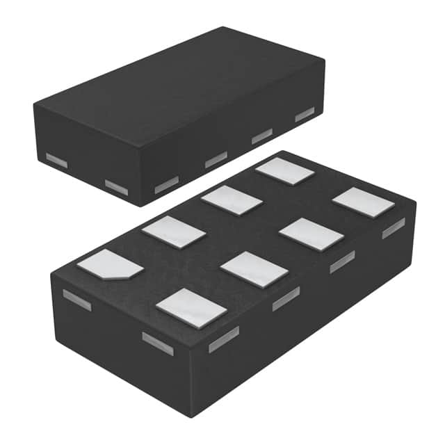
- Package: SOT753 (SC-70)
- Essence: Logic Level Translator
- Packaging/Quantity: Tape and Reel, 3000 pieces per reel
Specifications
- Supply Voltage Range: 1.65V to 5.5V
- Input Voltage Range: -0.5V to VCC + 0.5V
- Output Voltage Range: 0V to VCC
- Maximum Operating Frequency: 400 MHz
- Propagation Delay: 3.8 ns (typical)
- Output Drive Capability: ±24 mA
Detailed Pin Configuration
The 74LVC2G125GF,115 IC has a total of 6 pins: 1. Pin 1: A Input 2. Pin 2: Y Output 3. Pin 3: B Input 4. Pin 4: GND (Ground) 5. Pin 5: VCC (Supply Voltage) 6. Pin 6: OE (Output Enable)
Functional Features
- Dual non-inverting buffer with 3-state output
- Allows bidirectional voltage level translation between different logic levels
- Supports mixed-mode signal operation
- Provides protection against bus contention and overvoltage
- Low power consumption and high noise immunity
Advantages and Disadvantages
Advantages: - High-speed operation - Wide supply voltage range - Small package size - Low power consumption
Disadvantages: - Limited output drive capability - Not suitable for high-current applications
Working Principles
The 74LVC2G125GF,115 is designed to act as a buffer or driver in digital systems. It receives input signals from one logic level and translates them to another logic level, allowing seamless communication between different parts of a circuit. The IC operates by using internal transistors to amplify and shape the input signals, ensuring reliable and accurate data transmission.
Detailed Application Field Plans
The 74LVC2G125GF,115 is commonly used in various applications, including: 1. Microcontrollers and microprocessors 2. Communication systems 3. Industrial automation 4. Consumer electronics 5. Automotive electronics
Detailed and Complete Alternative Models
Some alternative models that can be used as replacements for the 74LVC2G125GF,115 include: - SN74LVC2G125DCUR - MC74VHC2G125DTT1G - TC7SZ125FU(TE85L,F)
These alternative models offer similar functionality and specifications, providing flexibility in design choices.
In conclusion, the 74LVC2G125GF,115 is a high-speed, low-power dual bus buffer IC used for logic level translation. It offers advantages such as wide supply voltage range and small package size. However, it has limitations in terms of output drive capability. With its various applications and alternative models available, this IC provides a versatile solution for digital systems.
Senaraikan 10 soalan dan jawapan biasa yang berkaitan dengan aplikasi 74LVC2G125GF,115 dalam penyelesaian teknikal
Sure! Here are 10 common questions and answers related to the application of 74LVC2G125GF,115 in technical solutions:
Q: What is the function of the 74LVC2G125GF,115? A: The 74LVC2G125GF,115 is a dual bus buffer gate with 3-state outputs. It can be used for level shifting and signal buffering.
Q: What is the operating voltage range of the 74LVC2G125GF,115? A: The operating voltage range is from 1.65V to 5.5V.
Q: Can the 74LVC2G125GF,115 handle high-speed signals? A: Yes, it has a high-speed operation capability with a maximum propagation delay of 4.3 ns.
Q: How many inputs and outputs does the 74LVC2G125GF,115 have? A: It has two inputs and two outputs.
Q: What is the output drive strength of the 74LVC2G125GF,115? A: The output drive strength is typically 24 mA.
Q: Can the 74LVC2G125GF,115 be used for bidirectional communication? A: No, it is a unidirectional buffer and cannot be used for bidirectional communication.
Q: Is the 74LVC2G125GF,115 compatible with both CMOS and TTL logic levels? A: Yes, it is compatible with both CMOS and TTL logic levels.
Q: What is the package type of the 74LVC2G125GF,115? A: It is available in a small SOT753 package.
Q: Can the 74LVC2G125GF,115 be used in automotive applications? A: Yes, it is AEC-Q100 qualified and suitable for automotive applications.
Q: Are there any recommended application circuits available for the 74LVC2G125GF,115? A: Yes, the datasheet of the component provides several recommended application circuits for different use cases.
Please note that the answers provided here are general and may vary depending on specific requirements and use cases. It is always recommended to refer to the datasheet and consult with technical experts for accurate information.