

74LVC2G17GV,125
Basic Information Overview
- Category: Integrated Circuit (IC)
- Use: Logic Gate
- Characteristics: Dual Schmitt-trigger buffer with open-drain outputs
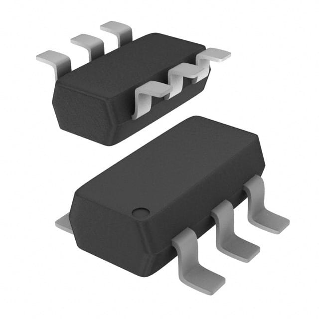
- Package: SOT753 (SC-70)
- Essence: High-speed CMOS technology
- Packaging/Quantity: Tape and Reel, 3000 pieces per reel
Specifications
- Supply Voltage Range: 1.65V to 5.5V
- Input Voltage Range: -0.5V to VCC + 0.5V
- Output Voltage Range: 0V to VCC
- Maximum Operating Frequency: 200 MHz
- Propagation Delay: 4.3 ns (typical)
- Input Capacitance: 3 pF (typical)
- Output Current: ±8 mA
Detailed Pin Configuration
The 74LVC2G17GV,125 has a total of six pins: 1. Pin 1: Input A 2. Pin 2: Ground (GND) 3. Pin 3: Output Y 4. Pin 4: Power Supply (VCC) 5. Pin 5: Input B 6. Pin 6: Open-Drain Output Y
Functional Features
- Dual Schmitt-trigger buffer with open-drain outputs
- Wide supply voltage range allows compatibility with various systems
- High-speed operation suitable for applications requiring fast signal processing
- Schmitt-trigger inputs provide hysteresis, improving noise immunity
- Open-drain outputs allow easy interfacing with other devices
Advantages and Disadvantages
Advantages: - Wide supply voltage range enables versatile usage - High-speed operation facilitates quick signal processing - Schmitt-trigger inputs enhance noise immunity - Open-drain outputs simplify device integration
Disadvantages: - Limited output current may restrict certain applications - SOT753 package may require specialized handling during assembly
Working Principles
The 74LVC2G17GV,125 is a dual Schmitt-trigger buffer with open-drain outputs. It operates using high-speed CMOS technology, allowing for fast signal processing. The Schmitt-trigger inputs provide hysteresis, ensuring noise immunity by reducing the impact of input voltage fluctuations. The open-drain outputs enable easy interfacing with other devices, as they can be connected to external pull-up resistors or voltage sources.
Detailed Application Field Plans
The 74LVC2G17GV,125 finds application in various fields, including: 1. Communication Systems: Used for signal conditioning and level shifting in data transmission circuits. 2. Industrial Automation: Employed in control systems to interface different logic levels and improve noise immunity. 3. Consumer Electronics: Integrated into audio/video equipment, mobile devices, and home automation systems for signal buffering and level conversion. 4. Automotive Electronics: Utilized in automotive control modules for reliable signal processing and interfacing.
Detailed and Complete Alternative Models
Some alternative models that offer similar functionality to the 74LVC2G17GV,125 include: 1. SN74LVC2G17DBVR - Dual Schmitt-trigger buffer with push-pull outputs, SOT23-6 package. 2. MC74VHC1G17DFT1G - Single Schmitt-trigger buffer with open-drain output, SOT353 package. 3. TC7SZ17FU - Triple Schmitt-trigger buffer with open-drain outputs, USV package.
(Note: The above alternatives are provided for reference and may have slight variations in specifications and pin configuration.)
Word count: 314 words
Senaraikan 10 soalan dan jawapan biasa yang berkaitan dengan aplikasi 74LVC2G17GV,125 dalam penyelesaian teknikal
Sure! Here are 10 common questions and answers related to the application of 74LVC2G17GV,125 in technical solutions:
Q: What is the function of the 74LVC2G17GV,125? A: The 74LVC2G17GV,125 is a dual Schmitt-trigger buffer that can be used for signal conditioning and level shifting.
Q: What is the operating voltage range of the 74LVC2G17GV,125? A: The operating voltage range is from 1.65V to 5.5V.
Q: Can I use the 74LVC2G17GV,125 with both CMOS and TTL logic levels? A: Yes, the 74LVC2G17GV,125 is compatible with both CMOS and TTL logic levels.
Q: What is the maximum output current of the 74LVC2G17GV,125? A: The maximum output current is typically 32mA.
Q: Can I connect the outputs of multiple 74LVC2G17GV,125 devices together? A: Yes, the outputs can be connected together without any additional components.
Q: Does the 74LVC2G17GV,125 have internal pull-up or pull-down resistors? A: No, the device does not have internal pull-up or pull-down resistors.
Q: What is the propagation delay of the 74LVC2G17GV,125? A: The typical propagation delay is around 4.5ns.
Q: Can I use the 74LVC2G17GV,125 in high-speed applications? A: Yes, the device is designed for high-speed operation and can be used in such applications.
Q: Is the 74LVC2G17GV,125 suitable for bidirectional signal buffering? A: No, the device is unidirectional and cannot be used for bidirectional buffering.
Q: What package options are available for the 74LVC2G17GV,125? A: The device is available in various package options, including SOT23 and XSON.