

74LVC2G241GM,125
Basic Information Overview
- Category: Integrated Circuit (IC)
- Use: Logic Gate Buffer/Driver
- Characteristics:
- Low-voltage CMOS technology
- Dual buffer/driver with 3-state outputs
- High-speed operation
- Wide operating voltage range
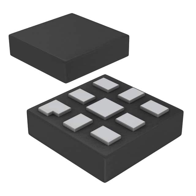
- Package: 8-pin VSSOP (Very Small Outline Package)
- Essence: Buffering and driving signals in digital circuits
- Packaging/Quantity: Tape and Reel, 3000 units per reel
Specifications
- Supply Voltage Range: 1.65V to 5.5V
- Input Voltage Range: 0V to VCC
- Output Voltage Range: 0V to VCC
- Operating Temperature Range: -40°C to +125°C
- Input Capacitance: 4.5pF
- Output Capacitance: 6pF
- Propagation Delay: 3.9ns (typical)
Detailed Pin Configuration
The 74LVC2G241GM,125 has the following pin configuration:
___________
   OE | 1       8 | VCC
 I/O1 | 2       7 | GND
  I/O | 3       6 | I/O2
  GND | 4       5 | OE#
       ‾‾‾‾‾‾‾‾‾‾‾
Functional Features
- Dual buffer/driver with independent control of each output
- 3-state outputs allow multiple devices to share a bus
- High-speed operation enables efficient signal transmission
- Low power consumption due to low-voltage CMOS technology
- Schmitt-trigger inputs for improved noise immunity
Advantages and Disadvantages
Advantages: - Wide operating voltage range allows compatibility with various systems - Small package size saves board space - 3-state outputs facilitate bus sharing in multi-device applications
Disadvantages: - Limited output current capability - Not suitable for high-power applications
Working Principles
The 74LVC2G241GM,125 is a buffer/driver IC that amplifies and shapes digital signals. It operates using low-voltage CMOS technology, which ensures low power consumption and compatibility with a wide range of supply voltages. The inputs are equipped with Schmitt-trigger circuitry to improve noise immunity. The 3-state outputs enable multiple devices to share a common bus, allowing efficient communication between different parts of a digital system.
Detailed Application Field Plans
The 74LVC2G241GM,125 finds application in various fields, including: 1. Microcontrollers and microprocessors 2. Communication systems 3. Industrial automation 4. Consumer electronics 5. Automotive electronics
In microcontroller-based systems, this IC can be used to buffer and drive signals between the microcontroller and other peripheral devices. In communication systems, it helps amplify and shape digital signals for transmission. In industrial automation, it enables interfacing between control units and actuators/sensors. In consumer electronics, it plays a role in signal conditioning and level shifting. In automotive electronics, it assists in signal buffering and driving within the vehicle's electronic systems.
Detailed and Complete Alternative Models
Some alternative models to the 74LVC2G241GM,125 include: - SN74LVC2G241DCUR - MC74LVC2G241DTG - TC7SZ241FK(TE85L,F)
These models offer similar functionality and characteristics, providing alternatives for designers based on availability, pricing, and specific application requirements.
Word count: 408 words
Senaraikan 10 soalan dan jawapan biasa yang berkaitan dengan aplikasi 74LVC2G241GM,125 dalam penyelesaian teknikal
Sure! Here are 10 common questions and answers related to the application of 74LVC2G241GM,125:
Q: What is the function of the 74LVC2G241GM,125? A: The 74LVC2G241GM,125 is a dual buffer/line driver IC that can be used for voltage level translation and signal buffering.
Q: What is the operating voltage range of the 74LVC2G241GM,125? A: The 74LVC2G241GM,125 operates within a voltage range of 1.65V to 5.5V.
Q: How many input/output pins does the 74LVC2G241GM,125 have? A: The 74LVC2G241GM,125 has two input pins and two output pins.
Q: Can the 74LVC2G241GM,125 be used for bidirectional communication? A: No, the 74LVC2G241GM,125 is unidirectional and can only be used for one-way signal transmission.
Q: What is the maximum data rate supported by the 74LVC2G241GM,125? A: The 74LVC2G241GM,125 supports a maximum data rate of 100 Mbps.
Q: Does the 74LVC2G241GM,125 have any built-in protection features? A: Yes, the 74LVC2G241GM,125 has built-in ESD protection on its inputs and outputs.
Q: Can the 74LVC2G241GM,125 be used in automotive applications? A: Yes, the 74LVC2G241GM,125 is AEC-Q100 qualified and suitable for automotive applications.
Q: What is the package type of the 74LVC2G241GM,125? A: The 74LVC2G241GM,125 is available in a small SOT753 package.
Q: Can the 74LVC2G241GM,125 be used in battery-powered devices? A: Yes, the 74LVC2G241GM,125 has low power consumption and can be used in battery-powered applications.
Q: Are there any recommended application circuits available for the 74LVC2G241GM,125? A: Yes, the datasheet of the 74LVC2G241GM,125 provides example application circuits that can be used as reference designs.
Please note that these answers are general and may vary depending on the specific requirements and use cases. It's always recommended to refer to the datasheet and consult with technical experts for accurate information.