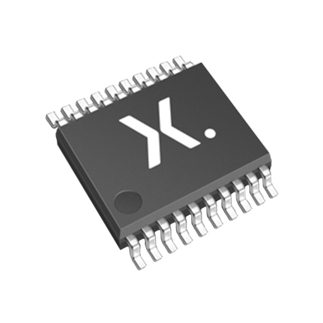
74LVT244BPW,118
Basic Information Overview
- Category: Integrated Circuit (IC)
- Use: Buffer/Line Driver
- Characteristics: Low Voltage, Tri-State Outputs
- Package: TSSOP (Thin Shrink Small Outline Package)
- Essence: High-Speed CMOS Octal Buffer/Line Driver with 3-State Outputs
- Packaging/Quantity: Tape and Reel, 2500 pieces per reel
Specifications
- Supply Voltage Range: 1.2V to 3.6V
- Input Voltage Range: 0V to VCC
- Output Voltage Range: 0V to VCC
- Maximum Operating Frequency: 200MHz
- Number of Channels: 8
- Output Current: ±24mA
- Propagation Delay Time: 4.5ns (Max) at 3.3V
- Operating Temperature Range: -40°C to +85°C
Detailed Pin Configuration
The 74LVT244BPW,118 IC has a total of 20 pins, which are assigned as follows:
- Pin 1: Output Enable (OE)
- Pin 2: Input/Output (IO1)
- Pin 3: Input/Output (IO2)
- Pin 4: Ground (GND)
- Pin 5: Input/Output (IO3)
- Pin 6: Input/Output (IO4)
- Pin 7: Input/Output (IO5)
- Pin 8: Input/Output (IO6)
- Pin 9: Power Supply (VCC)
- Pin 10: Input/Output (IO7)
- Pin 11: Input/Output (IO8)
- Pin 12: Output (Q1)
- Pin 13: Output (Q2)
- Pin 14: Output (Q3)
- Pin 15: Output (Q4)
- Pin 16: Output (Q5)
- Pin 17: Output (Q6)
- Pin 18: Output (Q7)
- Pin 19: Output (Q8)
- Pin 20: Ground (GND)
Functional Features
- High-Speed CMOS technology allows for fast switching times and low power consumption.
- Tri-State outputs provide flexibility in controlling the output state.
- Wide supply voltage range enables compatibility with various systems.
- ESD protection on all pins ensures robustness against electrostatic discharge.
Advantages and Disadvantages
Advantages: - High-speed operation suitable for demanding applications. - Low power consumption extends battery life in portable devices. - Tri-State outputs allow multiple devices to share a common bus. - ESD protection enhances reliability in harsh environments.
Disadvantages: - Limited output current may not be sufficient for driving heavy loads. - Narrow operating temperature range restricts usage in extreme conditions. - TSSOP package may require careful handling during assembly.
Working Principles
The 74LVT244BPW,118 is an octal buffer/line driver IC that amplifies and buffers digital signals. It operates using high-speed CMOS technology, which combines the advantages of both CMOS and TTL logic families. The inputs are compatible with TTL and CMOS voltage levels, making it versatile for interfacing with different logic families. The tri-state outputs allow the device to be connected to a common bus, enabling multiple devices to share the same communication lines.
Detailed Application Field Plans
The 74LVT244BPW,118 is commonly used in various applications, including but not limited to: - Data communication systems - Networking equipment - Industrial automation - Consumer electronics - Automotive electronics
Detailed and Complete Alternative Models
Some alternative models that can be considered as replacements or substitutes for the 74LVT244BPW,118 include: - SN74LVT244APWR - MC74LVT244ADWR2G - 74LVT244D,118 - CD74LVT244M96
These alternative models offer similar functionality and characteristics, but may differ in package type, pin configuration, or manufacturer.
Word count: 346 words
Senaraikan 10 soalan dan jawapan biasa yang berkaitan dengan aplikasi 74LVT244BPW,118 dalam penyelesaian teknikal
Sure! Here are 10 common questions and answers related to the application of 74LVT244BPW,118:
Q: What is the 74LVT244BPW,118? A: The 74LVT244BPW,118 is a octal buffer/line driver with 3-state outputs, commonly used in digital logic circuits.
Q: What is the maximum operating voltage for the 74LVT244BPW,118? A: The maximum operating voltage for this IC is typically 3.6V.
Q: How many inputs and outputs does the 74LVT244BPW,118 have? A: It has 8 inputs and 8 outputs.
Q: What is the purpose of the 3-state outputs in this IC? A: The 3-state outputs allow multiple devices to share a common bus without interfering with each other.
Q: Can the 74LVT244BPW,118 be used in both TTL and CMOS logic systems? A: Yes, it is compatible with both TTL and CMOS logic levels.
Q: What is the maximum output current that can be sourced or sunk by the 74LVT244BPW,118? A: The maximum output current is typically around 32mA.
Q: Is the 74LVT244BPW,118 capable of driving capacitive loads? A: Yes, it can drive capacitive loads up to a certain limit specified in the datasheet.
Q: Can I use the 74LVT244BPW,118 in high-speed applications? A: Yes, it is designed for high-speed operation and can be used in such applications.
Q: Does the 74LVT244BPW,118 have any built-in protection features? A: Yes, it has built-in ESD protection on all inputs and outputs.
Q: What is the package type of the 74LVT244BPW,118? A: It comes in a TSSOP-20 package.
Please note that these answers are general and may vary depending on the specific datasheet and manufacturer's specifications for the 74LVT244BPW,118.


