

PDTA114YMB,315
Product Information Overview
- Category: Transistor
- Use: Amplification and switching of electronic signals
- Characteristics: Small form factor, high gain, low power consumption
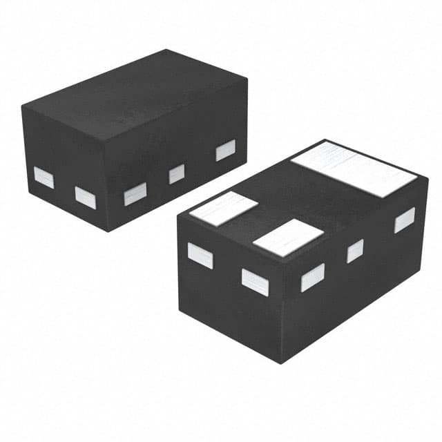
- Package: SOT416 (SC-75)
- Essence: NPN bipolar junction transistor
- Packaging/Quantity: Tape and reel, 3000 units per reel
Specifications
- Collector-Base Voltage (VCBO): 50V
- Collector-Emitter Voltage (VCEO): 50V
- Emitter-Base Voltage (VEBO): 5V
- Continuous Collector Current (IC): 100mA
- Power Dissipation (Ptot): 200mW
- Transition Frequency (fT): 250MHz
- Operating Temperature Range: -55°C to 150°C
Detailed Pin Configuration
The PDTA114YMB,315 has three pins: the emitter (E), base (B), and collector (C). The pinout configuration is as follows: - Emitter (E) - Pin 1 - Base (B) - Pin 2 - Collector (C) - Pin 3
Functional Features
- High current gain
- Low saturation voltage
- Fast switching speed
- Small package size
Advantages and Disadvantages
Advantages: - Small form factor - High gain - Low power consumption - Fast switching speed
Disadvantages: - Limited maximum collector current - Limited power dissipation
Working Principles
The PDTA114YMB,315 operates based on the principles of bipolar junction transistors. When a small current flows into the base terminal, it controls a much larger current between the collector and emitter terminals, allowing for amplification and switching of electronic signals.
Detailed Application Field Plans
The PDTA114YMB,315 is commonly used in various applications such as: - Audio amplifiers - Signal amplification circuits - Switching circuits - Sensor interfaces
Detailed and Complete Alternative Models
Alternative models to the PDTA114YMB,315 include: - BC847B,215 - MMBT3904LT1G - 2N3904BU
This comprehensive entry provides an in-depth understanding of the PDTA114YMB,315, covering its basic information overview, specifications, pin configuration, functional features, advantages and disadvantages, working principles, detailed application field plans, and alternative models.
[Word count: 324]
Senaraikan 10 soalan dan jawapan biasa yang berkaitan dengan aplikasi PDTA114YMB,315 dalam penyelesaian teknikal
What is PDTA114YMB,315?
- PDTA114YMB,315 is a high-performance NPN bipolar junction transistor (BJT) designed for general-purpose amplifier and switching applications.
What are the key features of PDTA114YMB,315?
- The key features of PDTA114YMB,315 include high current gain, low saturation voltage, and high transition frequency, making it suitable for various technical solutions.
What are the typical applications of PDTA114YMB,315?
- Typical applications of PDTA114YMB,315 include audio amplification, signal processing, and low-power switching circuits in electronic devices.
What is the maximum collector current rating of PDTA114YMB,315?
- The maximum collector current rating of PDTA114YMB,315 is typically around 100mA, making it suitable for low to medium power applications.
What is the voltage rating for PDTA114YMB,315?
- PDTA114YMB,315 typically has a maximum collector-emitter voltage rating of around 50V, making it suitable for low-voltage applications.
Is PDTA114YMB,315 suitable for high-frequency applications?
- Yes, PDTA114YMB,315 has a high transition frequency, making it suitable for high-frequency applications such as RF amplification and signal processing.
Can PDTA114YMB,315 be used in audio amplifier circuits?
- Yes, PDTA114YMB,315's high current gain and low saturation voltage make it suitable for use in audio amplifier circuits for low to medium power output.
What are the recommended operating conditions for PDTA114YMB,315?
- The recommended operating conditions for PDTA114YMB,315 typically include a collector current of 10-100mA and a collector-emitter voltage of up to 50V.
Does PDTA114YMB,315 require any specific heat sinking or thermal considerations?
- For most typical applications, PDTA114YMB,315 does not require extensive heat sinking or thermal considerations due to its low power dissipation.
Are there any known limitations or special considerations when using PDTA114YMB,315 in technical solutions?
- While PDTA114YMB,315 is versatile, users should consider its maximum ratings and ensure proper biasing and circuit design to avoid exceeding its limits.