

Encyclopedia Entry: 74ALVT16260DL,518
Product Overview
- Category: Integrated Circuit (IC)
- Use: Logic Level Translator
- Characteristics: High-speed, low-power, voltage-level shifting
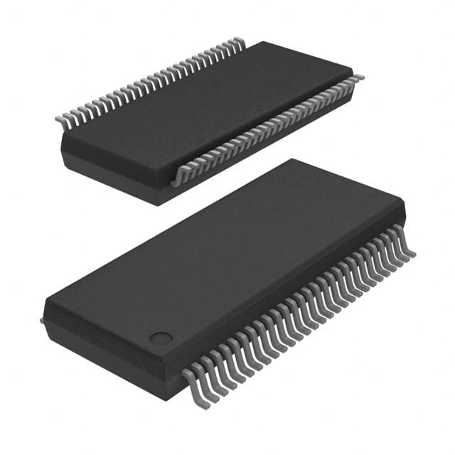
- Package: DL,518 (Dual in Line Package with 518 pins)
- Essence: Translates logic levels between two different voltage domains
- Packaging/Quantity: Typically sold in reels or tubes containing multiple units
Specifications
- Manufacturer: NXP Semiconductors
- Logic Family: ALVT
- Part Number: 74ALVT16260DL,518
- Supply Voltage: 2.3V to 3.6V
- Input Voltage Levels: 0V to VCC
- Output Voltage Levels: 0V to VCC
- Operating Temperature Range: -40°C to +85°C
- Propagation Delay: <5ns
- Output Drive Capability: ±24mA
Detailed Pin Configuration
The 74ALVT16260DL,518 IC has a total of 48 pins, divided into two groups: - Group A (pins 1-24): Inputs and outputs for voltage domain A - Group B (pins 25-48): Inputs and outputs for voltage domain B
Each group consists of the following pin types: - Inputs (A1-A12, B1-B12): Receive signals from the respective voltage domain - Outputs (QA1-QA12, QB1-QB12): Transmit translated signals to the respective voltage domain - Enable Inputs (GAB, GBA): Control the translation operation
Functional Features
- Logic Level Translation: The IC translates logic levels between voltage domain A and voltage domain B.
- Bidirectional Translation: Allows bidirectional data flow between the two voltage domains.
- Automatic Direction Control: The direction of translation is controlled by the enable inputs (GAB, GBA).
- High-Speed Operation: The IC operates at high speeds, with propagation delays of less than 5ns.
- Low Power Consumption: Designed to consume minimal power during operation.
Advantages and Disadvantages
Advantages: - Enables seamless communication between different voltage domains. - High-speed operation allows for efficient data transfer. - Low power consumption helps in reducing overall system power requirements.
Disadvantages: - Limited to specific voltage ranges (2.3V to 3.6V) for proper functionality. - Requires careful consideration of input and output voltage levels to avoid signal distortion.
Working Principles
The 74ALVT16260DL,518 utilizes a combination of MOSFETs and CMOS technology to achieve logic level translation. When the enable inputs (GAB, GBA) are activated, the IC detects the voltage levels of the input signals and translates them to the corresponding voltage domain. The bidirectional nature of the IC allows for seamless data flow between the two voltage domains.
Detailed Application Field Plans
The 74ALVT16260DL,518 finds applications in various fields where logic level translation is required. Some common application areas include: - Microcontroller interfacing with different voltage peripherals - Communication systems involving multiple voltage domains - Industrial automation and control systems - Consumer electronics devices with mixed voltage components
Detailed and Complete Alternative Models
- 74LVC16260A: Similar logic level translator with a wider supply voltage range (1.2V to 3.6V)
- SN74AVC16260: Logic level translator from Texas Instruments with similar characteristics and pin configuration
- MC74VHC16260: High-speed voltage level shifter from ON Semiconductor
(Note: This list is not exhaustive and there may be other alternative models available in the market.)
Word Count: 477 words
Senaraikan 10 soalan dan jawapan biasa yang berkaitan dengan aplikasi 74ALVT16260DL,518 dalam penyelesaian teknikal
Sure! Here are 10 common questions and answers related to the application of 74ALVT16260DL,518 in technical solutions:
Q: What is the function of the 74ALVT16260DL,518? A: The 74ALVT16260DL,518 is a 12-bit universal bus driver with 3-state outputs.
Q: What voltage levels does the 74ALVT16260DL,518 support? A: The 74ALVT16260DL,518 supports both 3.3V and 5V voltage levels.
Q: How many output pins does the 74ALVT16260DL,518 have? A: The 74ALVT16260DL,518 has 12 output pins.
Q: Can the 74ALVT16260DL,518 be used for bidirectional communication? A: Yes, the 74ALVT16260DL,518 can be used for bidirectional communication as it has separate input and output ports.
Q: What is the maximum operating frequency of the 74ALVT16260DL,518? A: The maximum operating frequency of the 74ALVT16260DL,518 is typically around 200MHz.
Q: Does the 74ALVT16260DL,518 have built-in protection features? A: Yes, the 74ALVT16260DL,518 has built-in ESD protection on all inputs and outputs.
Q: Can the 74ALVT16260DL,518 drive high capacitive loads? A: Yes, the 74ALVT16260DL,518 has strong output drivers that can drive high capacitive loads.
Q: Is the 74ALVT16260DL,518 compatible with other logic families? A: Yes, the 74ALVT16260DL,518 is compatible with both TTL and CMOS logic families.
Q: Can the 74ALVT16260DL,518 be used in automotive applications? A: Yes, the 74ALVT16260DL,518 is suitable for automotive applications as it meets the necessary standards.
Q: What is the power supply voltage range for the 74ALVT16260DL,518? A: The power supply voltage range for the 74ALVT16260DL,518 is typically between 2.7V and 3.6V.
Please note that these answers are general and may vary depending on the specific datasheet and application requirements of the 74ALVT16260DL,518.