

74HCT7403D,512
Basic Information Overview
- Category: Integrated Circuit (IC)
- Use: Logic Gate
- Characteristics: High-speed, low-power consumption
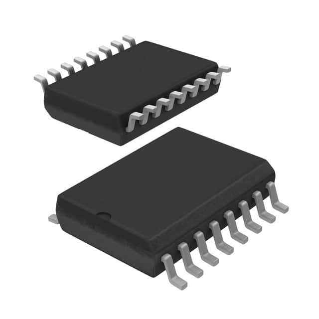
- Package: SOIC (Small Outline Integrated Circuit)
- Essence: Quad 2-input NAND gate
- Packaging/Quantity: Tape and Reel, 2500 pieces per reel
Specifications
- Supply Voltage Range: 2.0V to 6.0V
- Input Voltage Range: 0V to VCC
- Output Voltage Range: 0V to VCC
- Operating Temperature Range: -40°C to +125°C
- Propagation Delay Time: 10 ns (typical)
Detailed Pin Configuration
The 74HCT7403D,512 has a total of 14 pins. The pin configuration is as follows:
- A1 (Input A1)
- B1 (Input B1)
- Y1 (Output Y1)
- GND (Ground)
- A2 (Input A2)
- B2 (Input B2)
- Y2 (Output Y2)
- VCC (Supply Voltage)
- A3 (Input A3)
- B3 (Input B3)
- Y3 (Output Y3)
- NC (No Connection)
- A4 (Input A4)
- B4 (Input B4)
Functional Features
- Quad 2-input NAND gate with open-drain outputs
- Compatible with TTL levels
- Schmitt-trigger action on all inputs
- Balanced propagation delays
- Low power consumption
- High noise immunity
Advantages and Disadvantages
Advantages: - High-speed operation - Low power consumption - Wide supply voltage range - Schmitt-trigger action for improved noise immunity
Disadvantages: - Open-drain outputs may require additional pull-up resistors - Limited number of inputs and outputs
Working Principles
The 74HCT7403D,512 is a quad 2-input NAND gate with open-drain outputs. It operates by performing the logical NAND operation on the inputs A1/B1, A2/B2, A3/B3, and A4/B4. The output Y1/Y2/Y3 will be low (logic 0) only when both inputs are high (logic 1). The open-drain outputs allow for wired-OR connections and can be used to drive external devices.
Detailed Application Field Plans
The 74HCT7403D,512 can be used in various applications, including: - Digital logic circuits - Data processing systems - Communication systems - Industrial control systems - Automotive electronics
Detailed and Complete Alternative Models
Some alternative models that can be considered as replacements for the 74HCT7403D,512 are: - SN74HCT00N - CD4011BE - MC74HC00AN - 74LS00
These alternatives offer similar functionality and can be used interchangeably depending on the specific requirements of the application.
In conclusion, the 74HCT7403D,512 is a high-speed, low-power quad 2-input NAND gate IC. It offers balanced propagation delays, wide supply voltage range, and compatibility with TTL levels. Its open-drain outputs and Schmitt-trigger action make it suitable for various digital logic applications.
Senaraikan 10 soalan dan jawapan biasa yang berkaitan dengan aplikasi 74HCT7403D,512 dalam penyelesaian teknikal
Sure! Here are 10 common questions and answers related to the application of 74HCT7403D,512 in technical solutions:
Q: What is the function of the 74HCT7403D,512? A: The 74HCT7403D,512 is a quad 2-input NAND gate with open-drain outputs.
Q: What is the voltage supply range for this IC? A: The voltage supply range for the 74HCT7403D,512 is typically between 4.5V and 5.5V.
Q: Can I use this IC in a 3.3V system? A: Yes, the 74HCT7403D,512 is compatible with both 5V and 3.3V systems.
Q: How many gates are there in a single 74HCT7403D,512 package? A: There are four NAND gates in a single 74HCT7403D,512 package.
Q: What is the maximum output current of each gate? A: The maximum output current per gate is typically around 4mA.
Q: Can I connect the outputs of multiple gates together? A: Yes, you can connect the outputs of multiple gates together to create more complex logic functions.
Q: What is the propagation delay of the 74HCT7403D,512? A: The propagation delay is typically around 15ns.
Q: Can I use this IC in high-speed applications? A: Yes, the 74HCT7403D,512 is suitable for high-speed applications due to its low propagation delay.
Q: Is the 74HCT7403D,512 capable of driving capacitive loads? A: Yes, the outputs of this IC can drive capacitive loads up to a certain limit.
Q: Are there any special considerations for PCB layout when using this IC? A: It is recommended to follow proper PCB layout guidelines to minimize noise and ensure signal integrity.
Please note that these answers are general and may vary depending on specific application requirements.