

Encyclopedia Entry: 74F676PC
Product Information Overview
- Category: Integrated Circuit (IC)
- Use: Digital Logic Device
- Characteristics: High-speed, octal D-type flip-flop with common clock and reset
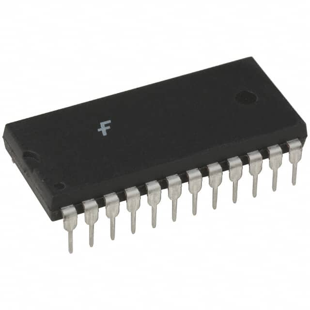
- Package: Plastic Dual In-Line Package (PDIP)
- Essence: Flip-flops are fundamental building blocks in digital circuits, used for storing and transferring binary data.
- Packaging/Quantity: Typically sold in reels or tubes containing multiple units.
Specifications
- Logic Family: 74F
- Number of Flip-Flops: 8 (octal)
- Clock Type: Common Clock
- Reset Type: Asynchronous Reset
- Operating Voltage: 5V
- Propagation Delay: 6 ns (typical)
- Input/Output Compatibility: TTL-compatible
Detailed Pin Configuration
The 74F676PC has a total of 20 pins. The pin configuration is as follows:
- D0 (Data Input 0)
- D1 (Data Input 1)
- D2 (Data Input 2)
- D3 (Data Input 3)
- D4 (Data Input 4)
- D5 (Data Input 5)
- D6 (Data Input 6)
- D7 (Data Input 7)
- GND (Ground)
- Q0 (Flip-Flop Output 0)
- Q1 (Flip-Flop Output 1)
- Q2 (Flip-Flop Output 2)
- Q3 (Flip-Flop Output 3)
- Q4 (Flip-Flop Output 4)
- Q5 (Flip-Flop Output 5)
- Q6 (Flip-Flop Output 6)
- Q7 (Flip-Flop Output 7)
- MR (Master Reset)
- CLK (Clock Input)
- VCC (Power Supply)
Functional Features
- Octal D-type flip-flop with common clock and reset functionality.
- Each flip-flop can store a single bit of binary data.
- Data is transferred to the outputs on the rising edge of the clock signal.
- Asynchronous master reset allows for clearing all flip-flops simultaneously.
Advantages and Disadvantages
Advantages: - High-speed operation suitable for time-critical applications. - TTL-compatible inputs and outputs ensure compatibility with other digital logic devices. - Asynchronous reset feature provides flexibility in system design.
Disadvantages: - Limited number of flip-flops (8) may not be sufficient for complex applications. - Power consumption may be relatively high compared to newer, low-power ICs.
Working Principles
The 74F676PC operates based on the principles of sequential logic. It consists of eight individual D-type flip-flops that share a common clock and reset signal. The flip-flops store binary data and transfer it to the outputs upon receiving a clock pulse. The asynchronous master reset allows for clearing all flip-flops simultaneously, regardless of the clock signal.
Detailed Application Field Plans
The 74F676PC is commonly used in various digital systems and applications, including:
- Microprocessor-based systems
- Data storage and retrieval systems
- Communication equipment
- Industrial control systems
- Test and measurement instruments
Detailed and Complete Alternative Models
Some alternative models that offer similar functionality to the 74F676PC include:
- 74LS676: Low-power version of the octal D-type flip-flop.
- 74HC676: High-speed CMOS version with TTL-compatible inputs and outputs.
- 74ACT676: Advanced CMOS version with improved speed and lower power consumption.
These alternative models can be considered based on specific application requirements and design constraints.
Word count: 346 words
Senaraikan 10 soalan dan jawapan biasa yang berkaitan dengan aplikasi 74F676PC dalam penyelesaian teknikal
Sure! Here are 10 common questions and answers related to the application of 74F676PC in technical solutions:
Q: What is the 74F676PC? A: The 74F676PC is a quad latch with transparent inputs and complementary outputs, commonly used in digital circuits.
Q: What is the purpose of the 74F676PC in technical solutions? A: The 74F676PC is used to store and control data in digital systems, providing latching functionality.
Q: How many latch units are there in the 74F676PC? A: The 74F676PC consists of four independent latch units, allowing for multiple data storage and control operations.
Q: What is the maximum operating frequency of the 74F676PC? A: The maximum operating frequency of the 74F676PC is typically around 100 MHz, but it can vary depending on the specific implementation.
Q: Can the 74F676PC be used in both synchronous and asynchronous applications? A: Yes, the 74F676PC can be used in both synchronous and asynchronous applications, depending on the design requirements.
Q: What is the power supply voltage range for the 74F676PC? A: The 74F676PC operates within a power supply voltage range of 4.5V to 5.5V.
Q: Does the 74F676PC support bidirectional data transfer? A: No, the 74F676PC only supports unidirectional data transfer from input to output.
Q: Can the 74F676PC be cascaded to increase the number of latch units? A: Yes, multiple 74F676PC devices can be cascaded together to increase the number of latch units in a system.
Q: What is the typical propagation delay of the 74F676PC? A: The typical propagation delay of the 74F676PC is around 10 ns, but it can vary depending on the specific operating conditions.
Q: Are there any special considerations for PCB layout when using the 74F676PC? A: Yes, it is important to follow proper PCB layout guidelines to minimize noise and ensure signal integrity when using the 74F676PC.
Please note that these answers are general and may vary depending on the specific implementation and datasheet of the 74F676PC.