

74LCX16374MEAX
Product Overview
- Category: Integrated Circuit (IC)
- Use: Flip-Flop
- Characteristics: Low-voltage, high-speed, and low-power consumption
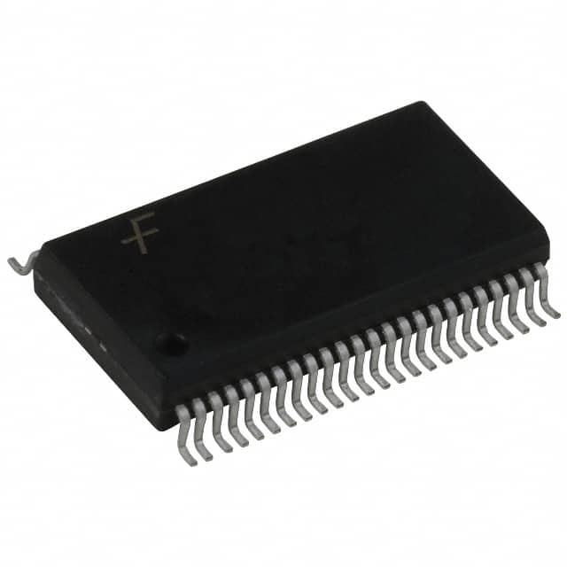
- Package: 48-pin TSSOP (Thin Shrink Small Outline Package)
- Essence: Sequential logic device for storing and transferring data
- Packaging/Quantity: Available in reels of 2500 units
Specifications
- Logic Family: LCX
- Number of Flip-Flops: 16
- Input Voltage Range: 2.0V to 3.6V
- Output Voltage Range: 0V to VCC
- Maximum Clock Frequency: 200MHz
- Propagation Delay: 2.5ns (max)
- Operating Temperature Range: -40°C to +85°C
Detailed Pin Configuration
The 74LCX16374MEAX has a total of 48 pins, which are assigned specific functions. The pin configuration is as follows:
- Pin 1: Data Input (D0)
- Pin 2: Data Input (D1)
- Pin 3: Data Input (D2)
- Pin 4: Data Input (D3)
- Pin 5: Data Input (D4)
- Pin 6: Data Input (D5)
- Pin 7: Data Input (D6)
- Pin 8: Data Input (D7)
- Pin 9: Data Input (D8)
- Pin 10: Data Input (D9)
- Pin 11: Data Input (D10)
- Pin 12: Data Input (D11)
- Pin 13: Data Input (D12)
- Pin 14: Data Input (D13)
- Pin 15: Data Input (D14)
- Pin 16: Data Input (D15)
- Pin 17: Clock Input (CP)
- Pin 18: Clock Enable Input (CE)
- Pin 19: Output Enable Input (OE)
- Pin 20: Master Reset Input (MR)
- Pin 21: Q0 Output
- Pin 22: Q1 Output
- Pin 23: Q2 Output
- Pin 24: Q3 Output
- Pin 25: Q4 Output
- Pin 26: Q5 Output
- Pin 27: Q6 Output
- Pin 28: Q7 Output
- Pin 29: Q8 Output
- Pin 30: Q9 Output
- Pin 31: Q10 Output
- Pin 32: Q11 Output
- Pin 33: Q12 Output
- Pin 34: Q13 Output
- Pin 35: Q14 Output
- Pin 36: Q15 Output
- Pin 37: GND (Ground)
- Pin 38: GND (Ground)
- Pin 39: VCC (Power Supply)
- Pin 40: VCC (Power Supply)
Functional Features
- The 74LCX16374MEAX is a 16-bit flip-flop with transparent latch and 3-state outputs.
- It operates at low voltage levels, making it suitable for battery-powered devices.
- The device offers high-speed performance, enabling efficient data transfer.
- It consumes low power, contributing to energy-efficient designs.
- The 3-state outputs allow multiple devices to share a common bus without interference.
Advantages and Disadvantages
Advantages: - Low-voltage operation extends battery life in portable applications. - High-speed performance enables quick data processing. - Low power consumption reduces energy requirements. - 3-state outputs facilitate bus sharing in complex systems.
Disadvantages: - Limited to 16-bit data storage and transfer. - Requires careful handling due to small package size.
Working Principles
The 74LCX16374MEAX operates based on the principles of sequential logic. It consists of 16 flip-flops that can store and transfer data. The device has a clock input (CP) that controls the timing of data transfer. When the clock signal transitions from low to high, the data present at the inputs (D0-D15) is latched and transferred to the corresponding outputs (Q0-Q15). The transparent latch feature allows continuous data flow when the clock enable input (CE) is high. The output enable input (OE) enables or disables the 3-state outputs. The master reset input (MR) resets all flip-flops to a known state when activated.
Detailed Application Field Plans
The 74LCX16374MEAX finds applications in various fields, including:
- Communication Systems: Used for data buffering and synchronization in communication protocols.
Senaraikan 10 soalan dan jawapan biasa yang berkaitan dengan aplikasi 74LCX16374MEAX dalam penyelesaian teknikal
Sure! Here are 10 common questions and answers related to the application of 74LCX16374MEAX in technical solutions:
Q: What is the 74LCX16374MEAX? A: The 74LCX16374MEAX is a 16-bit D-type flip-flop with 3-state outputs, designed for low-voltage applications.
Q: What is the operating voltage range of the 74LCX16374MEAX? A: The operating voltage range is typically between 2.0V and 3.6V.
Q: What is the maximum clock frequency supported by the 74LCX16374MEAX? A: The maximum clock frequency is typically around 200 MHz.
Q: Can I use the 74LCX16374MEAX in both synchronous and asynchronous applications? A: Yes, the 74LCX16374MEAX can be used in both synchronous and asynchronous applications.
Q: How many flip-flops are there in the 74LCX16374MEAX? A: The 74LCX16374MEAX has 16 flip-flops, hence the "16-bit" designation.
Q: What are the 3-state outputs used for? A: The 3-state outputs allow multiple devices to share a common bus without interfering with each other.
Q: Can I cascade multiple 74LCX16374MEAX devices together? A: Yes, you can cascade multiple devices to increase the number of flip-flops or create larger registers.
Q: What is the power consumption of the 74LCX16374MEAX? A: The power consumption is typically low due to its low-voltage design, but it can vary depending on the operating conditions.
Q: Can I use the 74LCX16374MEAX in battery-powered applications? A: Yes, the low-voltage design makes it suitable for battery-powered applications where power efficiency is important.
Q: Are there any specific precautions to consider when using the 74LCX16374MEAX? A: It is important to ensure proper voltage levels and signal integrity to avoid any potential issues with the device's performance.
Please note that these answers are general and may vary depending on the specific datasheet and manufacturer guidelines for the 74LCX16374MEAX.