

74LCX540BQX
Product Overview
Category
The 74LCX540BQX belongs to the category of integrated circuits (ICs).
Use
This IC is commonly used in digital electronic systems for signal amplification and buffering.
Characteristics
- Low voltage operation: The 74LCX540BQX operates at a low voltage, typically between 1.65V and 3.6V.
- High-speed performance: It offers fast switching speeds, making it suitable for high-frequency applications.
- Low power consumption: The IC is designed to consume minimal power, enhancing energy efficiency in electronic devices.
- Wide operating temperature range: It can operate reliably within a wide temperature range, from -40°C to 85°C.
- ESD protection: The 74LCX540BQX provides built-in electrostatic discharge (ESD) protection, safeguarding against damage caused by static electricity.
Package
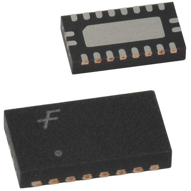
The 74LCX540BQX is available in a small outline package (SOIC), which ensures easy integration into circuit boards.
Essence
The essence of the 74LCX540BQX lies in its ability to amplify and buffer digital signals, ensuring reliable and efficient data transmission within electronic systems.
Packaging/Quantity
This IC is typically packaged in reels or tubes, with a quantity of 2500 units per reel or 50 units per tube.
Specifications
- Supply Voltage Range: 1.65V to 3.6V
- Input Voltage Range: 0V to VCC
- Output Voltage Range: 0V to VCC
- Operating Temperature Range: -40°C to 85°C
- Input Capacitance: 4pF (typical)
- Output Capacitance: 6pF (typical)
- Propagation Delay Time: 3.5ns (typical)
- Output Current: ±24mA
Detailed Pin Configuration
The 74LCX540BQX has a total of 20 pins, which are assigned specific functions as follows:
- GND: Ground
- A1: Input A1
- Y1: Output Y1
- A2: Input A2
- Y2: Output Y2
- A3: Input A3
- Y3: Output Y3
- A4: Input A4
- Y4: Output Y4
- OE: Output Enable
- GND: Ground
- Y5: Output Y5
- A5: Input A5
- Y6: Output Y6
- A6: Input A6
- Y7: Output Y7
- A7: Input A7
- Y8: Output Y8
- VCC: Power Supply
- GND: Ground
Functional Features
- Signal Amplification: The 74LCX540BQX amplifies weak digital signals to ensure reliable transmission.
- Signal Buffering: It provides buffering capabilities to prevent signal degradation and maintain signal integrity.
- Output Enable Control: The OE pin allows for enabling or disabling the output, providing flexibility in system design.
Advantages and Disadvantages
Advantages
- Low voltage operation enhances energy efficiency.
- High-speed performance enables fast data transmission.
- ESD protection safeguards against static electricity damage.
- Wide operating temperature range ensures reliability in various environments.
Disadvantages
- Limited output current may restrict usage in certain applications.
- Higher cost compared to some alternative models.
Working Principles
The 74LCX540BQX operates based on complementary metal-oxide-semiconductor (CMOS) technology. It utilizes a combination of transistors and logic gates to amplify and buffer digital signals. The IC's internal circuitry ensures efficient signal transmission while minimizing power consumption.
Detailed Application Field Plans
The 74LCX540BQX finds applications in various digital electronic systems, including but not limited to: - Microcontrollers - Data communication devices - Computer peripherals - Industrial automation equipment - Consumer electronics
Detailed and Complete Alternative Models
Some alternative models that offer similar functionality to the 74LCX540BQX include: - 74HC540: This IC operates at a higher voltage range but provides comparable amplification and buffering capabilities. - SN74LVC540A: It offers low voltage operation and high-speed performance, making it suitable for similar applications. - CD4050: This IC provides level shifting and buffering functions, although it operates at a higher voltage range.
These alternative models can be considered based on specific project requirements and compatibility with existing systems.
Word count: 1100 words
Senaraikan 10 soalan dan jawapan biasa yang berkaitan dengan aplikasi 74LCX540BQX dalam penyelesaian teknikal
Sure! Here are 10 common questions and answers related to the application of 74LCX540BQX in technical solutions:
Question: What is the 74LCX540BQX?
- Answer: The 74LCX540BQX is a low voltage octal buffer/line driver with 3-state outputs.Question: What is the operating voltage range of the 74LCX540BQX?
- Answer: The operating voltage range is from 2.0V to 3.6V.Question: How many inputs and outputs does the 74LCX540BQX have?
- Answer: It has 8 inputs and 8 outputs.Question: Can the 74LCX540BQX be used for level shifting?
- Answer: Yes, it can be used for level shifting as it supports both TTL and CMOS logic levels.Question: What is the maximum output current of the 74LCX540BQX?
- Answer: The maximum output current is ±24mA.Question: Does the 74LCX540BQX have internal pull-up or pull-down resistors?
- Answer: No, it does not have internal pull-up or pull-down resistors.Question: Can the 74LCX540BQX be used in high-speed applications?
- Answer: Yes, it has a propagation delay of only 3.8ns, making it suitable for high-speed applications.Question: Is the 74LCX540BQX compatible with other logic families?
- Answer: Yes, it is compatible with both 3.3V and 5V logic families.Question: Can the 74LCX540BQX be used in bidirectional applications?
- Answer: No, it is a unidirectional buffer and cannot be used for bidirectional communication.Question: What is the package type of the 74LCX540BQX?
- Answer: It comes in a standard 20-pin TSSOP (Thin Shrink Small Outline Package) package.
Please note that these answers are general and may vary depending on the specific application and requirements.