

74LCX74BQX
Product Overview
- Category: Integrated Circuit (IC)
- Use: Flip-Flop
- Characteristics: Low-voltage, low-power consumption, high-speed operation
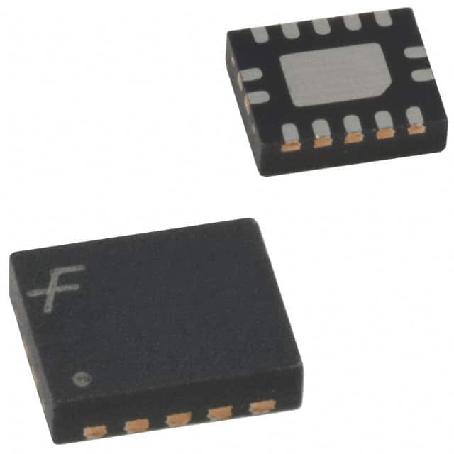
- Package: QFN (Quad Flat No-leads)
- Essence: Dual D-type flip-flop with set and reset
- Packaging/Quantity: Tape and Reel, 2500 units per reel
Specifications
- Supply Voltage: 1.65V to 3.6V
- Input Voltage Levels: CMOS/TTL compatible
- Operating Temperature Range: -40°C to +85°C
- Propagation Delay Time: 2.5ns (typical)
- Output Drive Capability: ±24mA
Pin Configuration
The 74LCX74BQX has a total of 14 pins, which are assigned as follows:
- Pin 1: Data Input A
- Pin 2: Clock Input A
- Pin 3: Set Input A
- Pin 4: Reset Input A
- Pin 5: Output A
- Pin 6: Ground (GND)
- Pin 7: Output B
- Pin 8: Data Input B
- Pin 9: Clock Input B
- Pin 10: Set Input B
- Pin 11: Reset Input B
- Pin 12: VCC (Supply Voltage)
- Pin 13: Clock Enable Input
- Pin 14: Clock Enable Output
Functional Features
- Dual D-type flip-flop with independent set and reset inputs
- High-speed operation, suitable for applications requiring fast data transfer
- Low-voltage operation allows compatibility with various systems
- CMOS/TTL compatible input voltage levels ensure easy integration with existing circuits
- Clock enable input and output for synchronization control
Advantages and Disadvantages
Advantages
- Low-voltage operation reduces power consumption
- High-speed operation enables efficient data processing
- Dual flip-flop design provides flexibility in circuit design
- Compatibility with CMOS/TTL input levels simplifies integration
Disadvantages
- Limited output drive capability may restrict use in certain applications
- Temperature range limited to -40°C to +85°C
Working Principles
The 74LCX74BQX is a dual D-type flip-flop that stores and transfers data based on clock signals. It features independent set and reset inputs, allowing the user to control the state of each flip-flop individually. The flip-flop operates at low voltages, making it suitable for various portable and battery-powered devices. The CMOS/TTL compatible input levels ensure seamless integration with different logic families.
Detailed Application Field Plans
The 74LCX74BQX finds applications in various fields, including:
- Digital communication systems
- Computer peripherals
- Consumer electronics
- Industrial automation
- Automotive electronics
- Medical equipment
Alternative Models
Below are some alternative models that can be considered as replacements for the 74LCX74BQX:
- SN74LVC74A: Dual positive-edge-triggered D-type flip-flop
- MC74LVX74: Dual D-type flip-flop with set and reset
- CD4013B: Dual D-type flip-flop with set and reset
These alternatives offer similar functionality and characteristics, providing options for different design requirements.
Word count: 348 words
Senaraikan 10 soalan dan jawapan biasa yang berkaitan dengan aplikasi 74LCX74BQX dalam penyelesaian teknikal
Sure! Here are 10 common questions and answers related to the application of 74LCX74BQX in technical solutions:
Question: What is the 74LCX74BQX?
- Answer: The 74LCX74BQX is a dual D-type flip-flop with set and reset inputs, designed for low-voltage operation.Question: What is the operating voltage range of the 74LCX74BQX?
- Answer: The 74LCX74BQX operates within a voltage range of 1.65V to 3.6V.Question: What is the maximum clock frequency supported by the 74LCX74BQX?
- Answer: The 74LCX74BQX can support clock frequencies up to 200MHz.Question: Can the 74LCX74BQX be used in battery-powered applications?
- Answer: Yes, the 74LCX74BQX is suitable for battery-powered applications due to its low-voltage operation.Question: How many flip-flops are there in the 74LCX74BQX?
- Answer: The 74LCX74BQX consists of two independent D-type flip-flops.Question: What is the typical propagation delay of the 74LCX74BQX?
- Answer: The typical propagation delay of the 74LCX74BQX is around 3.8ns.Question: Can the 74LCX74BQX be used in high-speed data transfer applications?
- Answer: Yes, the 74LCX74BQX is suitable for high-speed data transfer applications due to its fast propagation delay.Question: Does the 74LCX74BQX have any built-in protection features?
- Answer: Yes, the 74LCX74BQX has built-in ESD protection on all inputs and outputs.Question: Can the 74LCX74BQX be cascaded to create larger counters or shift registers?
- Answer: Yes, multiple 74LCX74BQX flip-flops can be cascaded to create larger counters or shift registers.Question: Is the 74LCX74BQX compatible with other logic families?
- Answer: The 74LCX74BQX is designed to be compatible with both 3.3V and 5V logic families, making it versatile for various applications.
Please note that these answers are general and may vary depending on specific application requirements.