

J111RL1G
Product Overview
- Category: Semiconductor
- Use: Amplification and switching of signals
- Characteristics: Low power, high gain, small package size
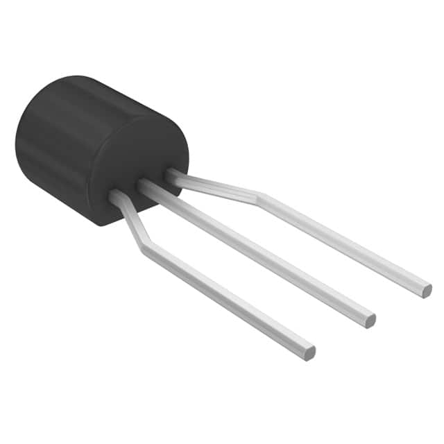
- Package: TO-92, SOT-23
- Essence: N-channel JFET
- Packaging/Quantity: Tape & Reel, 3000 units per reel
Specifications
- Maximum Drain-Source Voltage (Vds): 35V
- Maximum Gate-Source Voltage (Vgs): -25V
- Maximum Continuous Drain Current (Id): 50mA
- Maximum Power Dissipation (Pd): 350mW
- Transconductance (gm): 2.5mS
Detailed Pin Configuration
- Pin 1 (Gate): Input terminal for controlling the flow of current
- Pin 2 (Source): Connection to the ground or common reference point
- Pin 3 (Drain): Output terminal for the amplified or switched signal
Functional Features
- High input impedance
- Low noise
- Wide dynamic range
Advantages
- Simple biasing
- Low cost
- Minimal distortion
Disadvantages
- Susceptible to temperature variations
- Limited output swing
Working Principles
The J111RL1G operates based on the field effect principle, where the flow of current between the source and drain terminals is controlled by the voltage applied to the gate terminal.
Detailed Application Field Plans
- Audio amplifiers
- Instrumentation circuits
- Signal switching applications
Detailed and Complete Alternative Models
- J112RL1G
- J175RL1G
- 2N5457
This comprehensive entry provides a detailed understanding of the J111RL1G semiconductor, covering its specifications, pin configuration, functional features, advantages, disadvantages, working principles, application field plans, and alternative models.
Senaraikan 10 soalan dan jawapan biasa yang berkaitan dengan aplikasi J111RL1G dalam penyelesaian teknikal
Sure, here are 10 common questions and answers related to the application of J111RL1G in technical solutions:
What is J111RL1G?
- J111RL1G is a JFET (junction field-effect transistor) designed for general-purpose amplifier applications.
What are the key features of J111RL1G?
- The key features include low on-state resistance, high forward transfer admittance, and low input capacitance.
What are the typical applications of J111RL1G?
- Typical applications include low-frequency amplification, impedance matching, and signal switching.
What is the maximum drain-source voltage for J111RL1G?
- The maximum drain-source voltage is 35V.
What is the maximum continuous drain current for J111RL1G?
- The maximum continuous drain current is 25mA.
What is the input capacitance of J111RL1G?
- The input capacitance is typically 6pF.
What is the typical on-state resistance of J111RL1G?
- The typical on-state resistance is 25 ohms.
Can J111RL1G be used for audio amplifier applications?
- Yes, J111RL1G can be used for low-frequency audio amplifier applications.
What are the recommended operating temperature range for J111RL1G?
- The recommended operating temperature range is -55°C to 150°C.
Is J111RL1G suitable for battery-powered applications?
- Yes, J111RL1G is suitable for battery-powered applications due to its low power consumption and low on-state resistance.
I hope these questions and answers are helpful! Let me know if you need further assistance.