

MC74LVX259M
Overview
Category: Integrated Circuit (IC)
Use: Data Selector/Multiplexer
Characteristics: - Low-voltage CMOS technology - 8-bit multiplexer with 3-state outputs - Wide operating voltage range: 2.0V to 5.5V - High-speed operation: 20ns propagation delay - Low power consumption: 10µA maximum ICC - Available in SOIC package
Essence: The MC74LVX259M is a versatile integrated circuit that functions as an 8-bit data selector/multiplexer. It is designed using low-voltage CMOS technology, making it suitable for various applications requiring low power consumption and high-speed operation.
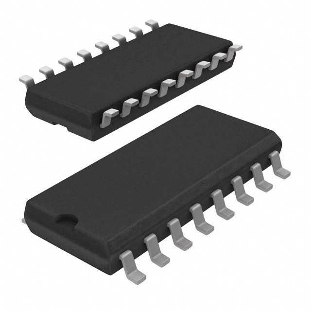
Packaging/Quantity: The MC74LVX259M is available in a Small Outline Integrated Circuit (SOIC) package. It is typically sold in reels or tubes containing multiple units.
Specifications
- Supply Voltage Range: 2.0V to 5.5V
- Input Voltage Range: 0V to VCC
- Output Voltage Range: 0V to VCC
- Operating Temperature Range: -40°C to +85°C
- Propagation Delay Time: 20ns (maximum)
- Input Capacitance: 3pF (typical)
- Output Capacitance: 6pF (typical)
- Power Dissipation: 500mW (maximum)
Pin Configuration
The MC74LVX259M has a total of 16 pins, which are assigned specific functions as follows:
- S0: Select Input 0
- S1: Select Input 1
- S2: Select Input 2
- G: Enable Input
- D0: Data Input 0
- D1: Data Input 1
- D2: Data Input 2
- D3: Data Input 3
- D4: Data Input 4
- D5: Data Input 5
- D6: Data Input 6
- D7: Data Input 7
- Q0: Output 0
- Q1: Output 1
- Q2: Output 2
- Q3: Output 3
Functional Features
The MC74LVX259M is primarily used as a data selector/multiplexer. It allows the selection of one out of eight input lines (D0-D7) to be routed to the outputs (Q0-Q3) based on the select inputs (S0-S2). The enable input (G) controls the output state, enabling or disabling the outputs.
Key functional features include: - High-speed operation with minimal propagation delay - Low power consumption, making it suitable for battery-powered devices - Wide operating voltage range, providing flexibility in various applications - 3-state outputs allow multiple devices to share a common bus
Advantages and Disadvantages
Advantages: - Low power consumption extends battery life in portable devices. - Wide operating voltage range enables compatibility with different systems. - High-speed operation facilitates efficient data processing. - 3-state outputs allow for easy bus sharing among multiple devices.
Disadvantages: - Limited number of input lines (8-bit). - Not suitable for applications requiring higher bit capacity. - May not be compatible with older CMOS technologies.
Working Principles
The MC74LVX259M operates based on the principles of digital multiplexing. The select inputs (S0-S2) determine which of the eight data inputs (D0-D7) will be selected and routed to the corresponding outputs (Q0-Q3). The enable input (G) controls the output state, enabling or disabling the outputs.
When the enable input is high, the selected data input is transferred to the outputs. When the enable input is low, the outputs are in a high-impedance state, effectively disconnecting them from the circuit.
Detailed Application Field Plans
The MC74LVX259M finds applications in various fields, including:
- Data communication systems
- Digital multiplexing/demultiplexing circuits
- Microcontroller-based systems
- Address decoding circuits
- Memory interfacing circuits
- Industrial control systems
- Automotive electronics
- Consumer electronics
Detailed and Complete Alternative Models
- SN74LVX259: Similar 8-bit data selector/multiplexer IC by Texas Instruments.
- CD74LVX259: 8-bit data selector/multiplexer IC by Texas Instruments with similar characteristics.
- 74HC259: 8-bit addressable latch/decoder IC by various manufacturers.
These alternative models offer similar functionality and can be used as substitutes for the MC74LVX259M
Senaraikan 10 soalan dan jawapan biasa yang berkaitan dengan aplikasi MC74LVX259M dalam penyelesaian teknikal
Sure! Here are 10 common questions and answers related to the application of MC74LVX259M in technical solutions:
Q: What is MC74LVX259M? A: MC74LVX259M is a 8-bit addressable latch with 3-state outputs, commonly used in digital systems.
Q: What is the operating voltage range for MC74LVX259M? A: The operating voltage range for MC74LVX259M is typically between 2.0V and 5.5V.
Q: How many addressable latches are there in MC74LVX259M? A: MC74LVX259M has 8 addressable latches, which can be controlled individually.
Q: What are the typical applications of MC74LVX259M? A: MC74LVX259M is commonly used in applications such as data storage, address decoding, and multiplexing.
Q: What is the maximum output current that MC74LVX259M can handle? A: MC74LVX259M can handle a maximum output current of 12mA per pin.
Q: Can MC74LVX259M be cascaded to increase the number of addressable latches? A: Yes, MC74LVX259M can be cascaded to increase the number of addressable latches in a system.
Q: Does MC74LVX259M have built-in protection against electrostatic discharge (ESD)? A: Yes, MC74LVX259M has built-in ESD protection, which helps to safeguard the device during handling and operation.
Q: What is the typical propagation delay of MC74LVX259M? A: The typical propagation delay of MC74LVX259M is around 6ns.
Q: Can MC74LVX259M operate in a high-speed digital system? A: Yes, MC74LVX259M is designed to operate in high-speed digital systems with its fast switching characteristics.
Q: Is MC74LVX259M available in different package options? A: Yes, MC74LVX259M is available in various package options such as SOIC, TSSOP, and PDIP, providing flexibility for different design requirements.
Please note that the answers provided here are general and may vary depending on specific datasheet specifications and application requirements.