

NB4N11MDTG
Product Overview
- Category: Integrated Circuit
- Use: Signal Conditioning and Level Shifting
- Characteristics:
- High-speed operation
- Low power consumption
- Small package size
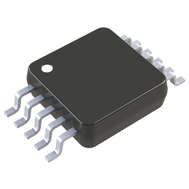
- Package: TSSOP-16
- Essence: Signal conditioning and level shifting for digital signals
- Packaging/Quantity: Tape and Reel, 2500 units per reel
Specifications
- Supply Voltage Range: 2.3V to 3.6V
- Input Voltage Range: 0V to VCC
- Output Voltage Range: 0V to VCC
- Operating Temperature Range: -40°C to +85°C
- Input Capacitance: 3pF (typical)
- Output Capacitance: 5pF (typical)
- Propagation Delay: 1.5ns (typical)
Detailed Pin Configuration
The NB4N11MDTG has a total of 16 pins arranged as follows:
```
| | | 1 2 3 | | | | 4 5 6 | | | | 7 8 9 | | | | 10 11 12 | | | | 13 14 15 | |_______________| ```
Pin Description: 1. VCC: Power supply voltage 2. GND: Ground reference 3. CLKIN: Clock input 4. CLKOUT: Clock output 5. LVCMOSIN: LVCMOS input 6. LVCMOSOUT: LVCMOS output 7. LVPECLIN: LVPECL input 8. LVPECLOUT: LVPECL output 9. LVDSIN: LVDS input 10. LVDSOUT: LVDS output 11. VREF: Reference voltage 12. SEL0: Select input 0 13. SEL1: Select input 1 14. NC: No connection 15. NC: No connection 16. NC: No connection
Functional Features
- Signal conditioning and level shifting for various digital signal types
- High-speed operation allows for reliable data transmission
- Low power consumption for energy-efficient applications
- Small package size enables space-saving designs
- Wide supply voltage range for versatile usage scenarios
Advantages and Disadvantages
Advantages: - High-speed operation ensures accurate signal processing - Low power consumption extends battery life in portable devices - Small package size facilitates compact circuit board designs
Disadvantages: - Limited pin configuration options may restrict certain applications - Sensitivity to voltage fluctuations may require additional voltage regulation measures
Working Principles
The NB4N11MDTG is designed to condition and shift the levels of digital signals. It accepts various input signal types, such as LVCMOS, LVPECL, and LVDS, and provides corresponding output signals at the desired voltage levels. The device operates by utilizing internal circuitry to amplify, filter, and adjust the timing characteristics of the input signals. This ensures reliable and accurate signal transmission between different components or systems.
Detailed Application Field Plans
The NB4N11MDTG can be used in a wide range of applications, including:
Communication Systems:
- Signal conditioning and level shifting in high-speed data communication interfaces.
- Integration into transceivers, routers, and switches for improved signal integrity.
Industrial Automation:
- Interface conversion between different logic families in control systems.
- Level shifting for sensor inputs and actuator outputs.
Automotive Electronics:
- Signal conditioning and level shifting in automotive communication networks.
- Integration into infotainment systems, advanced driver-assistance systems (ADAS), and engine control units (ECUs).
Consumer Electronics:
- Level shifting for display interfaces, such as LVDS to LVCMOS conversion.
- Signal conditioning for audio/video signals in home theater systems and multimedia devices.
Detailed and Complete Alternative Models
- SN74LVC1G34DBVR: Single Buffer/Driver with Open-Drain Output
- MC10EP16VADTG: Differential Receiver/Driver with LVPECL Outputs
- MAX9126ESE+: LVDS Line Driver/Receiver with Flow-Through Pinout
These alternative models offer similar functionality and can be considered as substitutes for the NB4N11MDTG in various applications.
Word count: 530 words
Senaraikan 10 soalan dan jawapan biasa yang berkaitan dengan aplikasi NB4N11MDTG dalam penyelesaian teknikal
Sure! Here are 10 common questions and answers related to the application of NB4N11MDTG in technical solutions:
Q: What is NB4N11MDTG? A: NB4N11MDTG is a high-performance differential receiver and driver IC used in various technical solutions.
Q: What are the key features of NB4N11MDTG? A: The key features of NB4N11MDTG include low jitter, wide operating voltage range, differential inputs/outputs, and compatibility with various signal standards.
Q: In what applications can NB4N11MDTG be used? A: NB4N11MDTG can be used in applications such as clock distribution, data transmission, signal conditioning, and clock/data recovery systems.
Q: What is the operating voltage range of NB4N11MDTG? A: NB4N11MDTG operates within a voltage range of typically 3.0V to 5.5V.
Q: Can NB4N11MDTG handle high-speed signals? A: Yes, NB4N11MDTG is designed to handle high-speed signals up to several gigabits per second (Gbps).
Q: Does NB4N11MDTG support multiple signal standards? A: Yes, NB4N11MDTG supports various signal standards such as LVDS, CML, LVPECL, HSTL, and SSTL.
Q: What is the input/output voltage swing of NB4N11MDTG? A: The input/output voltage swing of NB4N11MDTG is typically around 400mV to 800mV.
Q: Can NB4N11MDTG operate in harsh environments? A: Yes, NB4N11MDTG is designed to operate in a wide temperature range and can withstand harsh environmental conditions.
Q: Does NB4N11MDTG require external components for operation? A: Yes, NB4N11MDTG may require external components such as termination resistors and capacitors for proper operation.
Q: Is NB4N11MDTG readily available in the market? A: Availability may vary, but NB4N11MDTG is commonly stocked by various electronic component distributors and manufacturers.
Please note that the answers provided here are general and may vary depending on specific product specifications and application requirements.