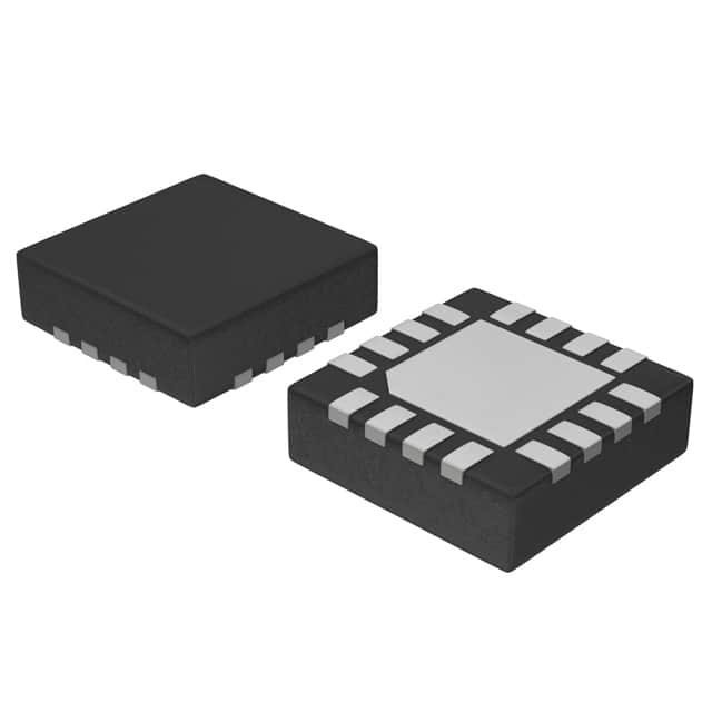
NB6L239MN
Basic Information Overview
- Category: Integrated Circuit (IC)
- Use: Clock and Data Distribution
- Characteristics:
- High-speed differential clock and data distribution
- Low additive phase noise
- Wide operating voltage range
- Small package size
- Package: QFN (Quad Flat No-leads)
- Essence: Efficient clock and data distribution solution
- Packaging/Quantity: Tape and Reel, 2500 units per reel
Specifications and Parameters
- Supply Voltage Range: 2.375V to 3.465V
- Input Voltage Range: -0.5V to VCC+0.5V
- Output Voltage Range: 0V to VCC
- Operating Temperature Range: -40°C to +85°C
- Maximum Input Clock Frequency: 2.7GHz
- Maximum Data Rate: 2.7Gbps
Detailed and Complete Pin Configuration
- CLKIN
- CLKINB
- VCC
- GND
- Q0
- Q0B
- Q1
- Q1B
- Q2
- Q2B
- Q3
- Q3B
- SEL
- OE#
Functional Characteristics
- Differential clock input with internal termination resistors
- Differential outputs with programmable output voltage swing
- Selectable output enable/disable function
- Internal biasing for improved noise performance
- ESD protection on all pins
Advantages and Disadvantages
Advantages: - High-speed clock and data distribution - Low phase noise - Wide operating voltage range - Compact package size
Disadvantages: - Limited maximum input clock frequency - Limited maximum data rate
Applicable Range of Products
- Communication systems
- Networking equipment
- Data centers
- High-speed digital systems
Working Principles
The NB6L239MN is designed to distribute high-speed clock and data signals in various applications. It accepts differential clock inputs and provides differential outputs with programmable voltage swing. The internal termination resistors ensure proper signal integrity. The device operates within a wide voltage range, making it suitable for different power supply configurations.
Detailed Application Field Plans
- Communication Systems: The NB6L239MN can be used to distribute clock and data signals in communication systems, ensuring accurate synchronization and reliable data transmission.
- Networking Equipment: In networking equipment, the IC can distribute clock signals to synchronize multiple devices, improving overall network performance.
- Data Centers: Clock distribution is critical in data centers to maintain synchronization between servers and storage systems. The NB6L239MN offers a compact and efficient solution for this purpose.
- High-Speed Digital Systems: The IC finds application in high-speed digital systems where precise clock distribution is essential for synchronous operation.
Detailed Alternative Models
- NB6L239MNG: Similar to NB6L239MN but with a different package option (TSSOP).
- NB6L239MNR2G: RoHS-compliant version of NB6L239MN.
- NB6L239MNTBG: Tape and reel packaging with 3000 units per reel.
5 Common Technical Questions and Answers
Q: What is the maximum input clock frequency supported by NB6L239MN? A: The maximum input clock frequency is 2.7GHz.
Q: Can I disable the output of the IC? A: Yes, the IC provides an output enable/disable function that can be controlled through the SEL pin.
Q: What is the operating temperature range of NB6L239MN? A: The IC can operate within a temperature range of -40°C to +85°C.
Q: Does NB6L239MN have built-in ESD protection? A: Yes, all pins of the IC are equipped with ESD protection.
Q: What is the recommended power supply voltage for NB6L239MN? A: The IC operates within a supply voltage range of 2.375V to 3.465V.
This encyclopedia entry provides an overview of the NB6L239MN integrated circuit, including its basic information, specifications, pin configuration, functional characteristics, advantages and disadvantages, applicable range of products, working principles, detailed application field plans, alternative models, and common technical questions and answers.


