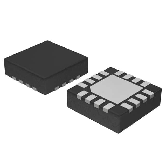
NB7L32MMNR2G
Basic Information Overview
- Category: Integrated Circuit (IC)
- Use: Logic Gate
- Characteristics: High-speed, Low-power consumption
- Package: QFN (Quad Flat No-leads)
- Essence: Dual Differential 2-Input OR/NOR Gate
- Packaging/Quantity: Tape & Reel, 3000 pieces per reel
Specifications and Parameters
- Supply Voltage: 1.8V to 3.3V
- Input Voltage Range: -0.5V to VCC + 0.5V
- Output Voltage Range: GND to VCC
- Operating Temperature Range: -40°C to +85°C
- Propagation Delay: 200ps (typical)
- Output Skew: 20ps (typical)
Detailed and Complete Pin Configuration
The NB7L32MMNR2G has a total of 16 pins arranged in a specific configuration: 1. Pin 1: VCC 2. Pin 2: IN1B 3. Pin 3: IN1A 4. Pin 4: GND 5. Pin 5: OUT1 6. Pin 6: /OE 7. Pin 7: NC 8. Pin 8: NC 9. Pin 9: NC 10. Pin 10: NC 11. Pin 11: NC 12. Pin 12: NC 13. Pin 13: OUT2 14. Pin 14: IN2A 15. Pin 15: IN2B 16. Pin 16: GND
Functional Characteristics
The NB7L32MMNR2G is a dual differential 2-input OR/NOR gate with the following functional characteristics: - High-speed operation - Low-power consumption - Compatible with various logic families - Differential inputs and outputs - Output enable/disable feature (/OE pin)
Advantages and Disadvantages
Advantages: - High-speed performance - Low-power consumption - Wide operating voltage range - Small package size
Disadvantages: - Limited number of input/output pins - Not suitable for all logic gate applications
Applicable Range of Products
The NB7L32MMNR2G is commonly used in electronic devices and systems that require high-speed logic operations, such as: - Data communication equipment - Networking devices - Test and measurement instruments - Industrial control systems
Working Principles
The NB7L32MMNR2G operates based on the principles of Boolean logic. It performs logical OR/NOR operations on its input signals and produces corresponding output signals.
Detailed Application Field Plans
The NB7L32MMNR2G can be applied in various fields, including: 1. Data transmission systems: Used to combine or negate multiple data signals. 2. Clock distribution networks: Used to generate clock signals with different phases. 3. Signal processing circuits: Used to perform logical operations on input signals. 4. Control systems: Used to implement decision-making functions based on input conditions. 5. Interface circuits: Used to interface between different logic families or voltage levels.
Detailed Alternative Models
Some alternative models to the NB7L32MMNR2G include: - SN74LVC1G32DBVR - MC74VHC1G32DTT1G - 74AUP1G32GW
5 Common Technical Questions and Answers
Q: What is the maximum supply voltage for the NB7L32MMNR2G? A: The maximum supply voltage is 3.3V.
Q: Can the NB7L32MMNR2G operate at temperatures below -40°C? A: Yes, the NB7L32MMNR2G has an operating temperature range of -40°C to +85°C.
Q: What is the typical propagation delay of the NB7L32MMNR2G? A: The typical propagation delay is 200ps.
Q: Does the NB7L32MMNR2G have an output enable/disable feature? A: Yes, the NB7L32MMNR2G has an output enable/disable pin (/OE).
Q: How many pins does the NB7L32MMNR2G have? A: The NB7L32MMNR2G has a total of 16 pins.
This encyclopedia entry provides detailed information about the NB7L32MMNR2G, including its product category, basic overview, specifications, pin configuration, functional characteristics, advantages and disadvantages, applicable range of products, working principles, application field plans, alternative models, and common technical questions and answers.


