

NBC12439AFNG
Basic Information Overview
- Category: Integrated Circuit (IC)
- Use: Digital Logic Device
- Characteristics:
- High-speed operation
- Low power consumption
- Compact size
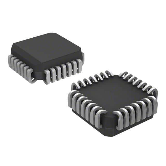
- Package: DIP-16 (Dual In-line Package, 16 pins)
- Essence: Logic gate IC for digital signal processing
- Packaging/Quantity: Tray packaging, 100 units per tray
Specifications and Parameters
- Supply Voltage: 3.3V - 5V
- Operating Temperature: -40°C to +85°C
- Input Voltage (High Level): 2.0V - Vcc
- Input Voltage (Low Level): GND - 0.8V
- Output Voltage (High Level): Vcc - 0.4V
- Output Voltage (Low Level): 0.4V
- Maximum Operating Frequency: 100 MHz
Detailed and Complete Pin Configuration
- A1: Input A1
- B1: Input B1
- Y1: Output Y1
- A2: Input A2
- B2: Input B2
- Y2: Output Y2
- GND: Ground
- Y3: Output Y3
- B3: Input B3
- A3: Input A3
- Y4: Output Y4
- B4: Input B4
- A4: Input A4
- Y5: Output Y5
- Vcc: Power Supply
- Y6: Output Y6
Functional Characteristics
- NBC12439AFNG is a 6-bit digital logic device that performs logical AND operations on its inputs.
- It has six independent AND gates with two inputs each.
- The output of each gate is determined by the logical AND operation of its inputs.
- The outputs are capable of driving standard TTL or CMOS logic levels.
Advantages and Disadvantages
Advantages: - High-speed operation allows for efficient digital signal processing. - Low power consumption reduces energy usage. - Compact size enables space-saving integration into electronic systems.
Disadvantages: - Limited to performing logical AND operations only. - Not suitable for applications requiring other logic functions, such as OR or NOT.
Applicable Range of Products
NBC12439AFNG is commonly used in various digital systems, including: - Microcontrollers - Digital signal processors - Communication devices - Industrial control systems
Working Principles
The NBC12439AFNG operates based on the principles of Boolean algebra. It performs logical AND operations on its input signals, producing corresponding output signals based on the truth table of the AND gate.
Detailed Application Field Plans
- Microcontroller-based Systems: Utilize NBC12439AFNG to perform logical AND operations for input/output control and data processing.
- Digital Signal Processors: Employ NBC12439AFNG to implement complex digital algorithms that require logical AND operations.
- Communication Devices: Integrate NBC12439AFNG to handle signal routing and filtering tasks.
- Industrial Control Systems: Incorporate NBC12439AFNG for logic-based decision-making processes.
Detailed Alternative Models
- NBC12438AFNG: 6-bit digital logic device with OR gate functionality.
- NBC12440AFNG: 6-bit digital logic device with XOR gate functionality.
- NBC12441AFNG: 6-bit digital logic device with NAND gate functionality.
- NBC12442AFNG: 6-bit digital logic device with NOR gate functionality.
- NBC12443AFNG: 6-bit digital logic device with XNOR gate functionality.
5 Common Technical Questions and Answers
Q: What is the maximum operating frequency of NBC12439AFNG? A: The maximum operating frequency is 100 MHz.
Q: Can NBC12439AFNG be powered with a voltage below 3.3V? A: No, the supply voltage should be within the range of 3.3V to 5V.
Q: How many inputs does each AND gate in NBC12439AFNG have? A: Each AND gate has two inputs.
Q: What is the output voltage range for a high-level signal? A: The output voltage for a high-level signal ranges from Vcc to 0.4V.
Q: Is NBC12439AFNG suitable for applications requiring logical OR operations? A: No, NBC12439AFNG can only perform logical AND operations.
This encyclopedia entry provides an overview of NBC12439AFNG, including its basic information, specifications, pin configuration, functional characteristics, advantages and disadvantages, applicable range of products, working principles, detailed application field plans, alternative models, and common technical questions and answers.