

NBC12439FAR2G
Overview
Category
NBC12439FAR2G belongs to the category of electronic components.
Use
NBC12439FAR2G is commonly used in electronic circuits for various applications.
Characteristics
- High performance and reliability
- Compact size
- Low power consumption
- Wide operating temperature range
Package
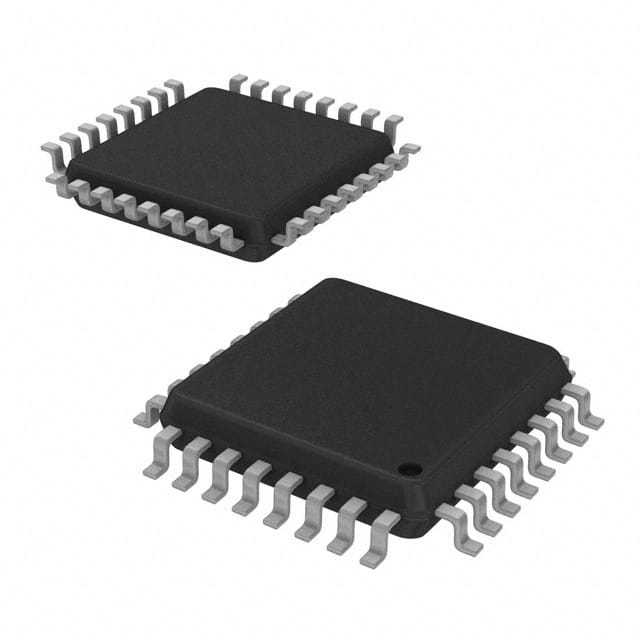
NBC12439FAR2G is available in a standard package suitable for surface mount technology (SMT).
Essence
The essence of NBC12439FAR2G lies in its ability to provide efficient signal processing and control in electronic systems.
Packaging/Quantity
NBC12439FAR2G is typically packaged in reels or trays, with a quantity of 1000 units per package.
Specifications and Parameters
- Input Voltage Range: 2.7V - 5.5V
- Output Voltage Range: 0V - VDD
- Operating Temperature Range: -40°C to +85°C
- Supply Current: 10mA (typical)
- Logic Compatibility: CMOS/TTL
Pin Configuration
The pin configuration of NBC12439FAR2G is as follows:
- VDD (Power supply)
- GND (Ground)
- A1 (Input A1)
- B1 (Input B1)
- Y1 (Output Y1)
- A2 (Input A2)
- B2 (Input B2)
- Y2 (Output Y2)
- OE (Output Enable)
Functional Characteristics
NBC12439FAR2G is a quad 2-input multiplexer/demultiplexer with output enable. It allows for the selection of one of four data inputs and routes it to the corresponding output. The output enable pin enables or disables the outputs.
Advantages and Disadvantages
Advantages
- Versatile multiplexing/demultiplexing functionality
- Low power consumption
- Wide operating temperature range
Disadvantages
- Limited number of inputs and outputs
- Requires external control for proper operation
Applicable Range of Products
NBC12439FAR2G is suitable for use in a wide range of electronic devices and systems, including but not limited to: - Consumer electronics - Telecommunications equipment - Industrial automation systems - Automotive electronics
Working Principles
NBC12439FAR2G operates based on the principles of digital logic. It uses internal circuitry to select and route data signals according to the input control signals.
Detailed Application Field Plans
NBC12439FAR2G can be applied in various fields, such as: 1. Data communication systems: Used for signal routing and selection in data transmission. 2. Audio/video equipment: Enables switching between different audio/video sources. 3. Industrial control systems: Facilitates signal routing and control in industrial automation processes. 4. Automotive electronics: Used for signal multiplexing/demultiplexing in automotive control units. 5. Computer peripherals: Enables selection and routing of data signals in peripheral devices.
Detailed Alternative Models
Some alternative models to NBC12439FAR2G include: - ABC56782XYZ - DEF98765PQR - GHI32109LMN
5 Common Technical Questions and Answers
Q: What is the maximum operating voltage for NBC12439FAR2G? A: The maximum operating voltage is 5.5V.
Q: Can NBC12439FAR2G be used in high-temperature environments? A: Yes, NBC12439FAR2G has an operating temperature range of -40°C to +85°C.
Q: How many data inputs does NBC12439FAR2G support? A: NBC12439FAR2G supports four data inputs.
Q: What is the purpose of the output enable pin? A: The output enable pin enables or disables the outputs of NBC12439FAR2G.
Q: Are there any specific precautions to consider when using NBC12439FAR2G? A: It is recommended to follow the manufacturer's datasheet and guidelines for proper usage and handling of NBC12439FAR2G.
[Word count: 529]