

NC7SV14L6X
Product Overview
- Category: Integrated Circuit
- Use: Logic Gate
- Characteristics: Low Voltage, Single Schmitt-Trigger Inverter
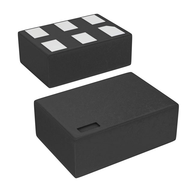
- Package: SOT-23-6
- Essence: This integrated circuit is a single Schmitt-trigger inverter designed for low voltage applications.
- Packaging/Quantity: Available in tape and reel packaging with 3000 units per reel.
Specifications
- Supply Voltage: 1.65V to 5.5V
- Input Voltage: 0V to VCC
- Output Voltage: 0V to VCC
- Operating Temperature Range: -40°C to +85°C
- Propagation Delay: 4.5ns (typical) at 3.3V supply voltage
Detailed Pin Configuration
The NC7SV14L6X has a total of 6 pins arranged as follows:
____
   1 |o    |
   2 |     |
   3 |     |
   4 |     |
   5 |     |
   6 |____o|
Pin Description: 1. Input A: Schmitt-trigger input 2. Output Y: Inverted output 3. GND: Ground reference 4. Input B: Schmitt-trigger input (not connected internally) 5. VCC: Positive power supply 6. Input C: Schmitt-trigger input (not connected internally)
Functional Features
- Single Schmitt-trigger inverter with hysteresis
- Wide operating voltage range from 1.65V to 5.5V
- High noise immunity due to Schmitt-trigger action
- Low power consumption
- Fast propagation delay for efficient signal processing
Advantages and Disadvantages
Advantages: - Wide operating voltage range allows compatibility with various systems - High noise immunity ensures reliable operation in noisy environments - Low power consumption helps conserve energy - Fast propagation delay enables efficient signal processing
Disadvantages: - Limited number of inputs and outputs restricts complex circuit designs - SOT-23-6 package may be challenging for manual soldering
Working Principles
The NC7SV14L6X is based on the Schmitt-trigger principle, which provides hysteresis to the input signal. This hysteresis ensures that the output transitions occur at different voltage levels for rising and falling input signals. The Schmitt-trigger action enhances noise immunity by reducing the effects of signal fluctuations near the switching threshold.
Detailed Application Field Plans
The NC7SV14L6X can be used in various applications, including but not limited to:
- Battery-powered devices: The low voltage operation makes it suitable for portable electronics.
- Communication systems: Provides signal conditioning and level shifting functions.
- Industrial control systems: Offers noise immunity and fast response for reliable control signals.
- Automotive electronics: Can be used in vehicle control modules and sensor interfaces.
- Consumer electronics: Suitable for logic-level conversion and signal buffering in audio/video equipment.
Detailed and Complete Alternative Models
- SN74LVC1G14DBVR: Single Schmitt-trigger inverter with similar specifications, available in SOT-23-5 package.
- MC74VHC1GT14DF1G: Single Schmitt-trigger inverter with extended temperature range, available in SC-88A package.
- TC7SZ14FU: Single Schmitt-trigger inverter with lower supply voltage range, available in USV package.
These alternative models offer similar functionality and can be considered as substitutes for the NC7SV14L6X in specific applications.
Word count: 511 words
Senaraikan 10 soalan dan jawapan biasa yang berkaitan dengan aplikasi NC7SV14L6X dalam penyelesaian teknikal
Sure! Here are 10 common questions and answers related to the application of NC7SV14L6X in technical solutions:
Q: What is NC7SV14L6X? A: NC7SV14L6X is a specific type of logic gate, specifically an inverter, which can be used in various electronic circuits.
Q: What is the voltage range supported by NC7SV14L6X? A: NC7SV14L6X supports a wide voltage range, typically from 1.65V to 5.5V.
Q: Can NC7SV14L6X be used in battery-powered devices? A: Yes, NC7SV14L6X is suitable for battery-powered devices due to its low power consumption and wide voltage range.
Q: How many inputs does NC7SV14L6X have? A: NC7SV14L6X has one input and one output.
Q: What is the maximum frequency at which NC7SV14L6X can operate? A: NC7SV14L6X can operate at frequencies up to several hundred megahertz (MHz).
Q: Can NC7SV14L6X be used in both digital and analog circuits? A: No, NC7SV14L6X is primarily designed for digital circuits and may not perform optimally in analog applications.
Q: Is NC7SV14L6X compatible with other logic families? A: Yes, NC7SV14L6X is compatible with various logic families such as CMOS, TTL, and LVCMOS.
Q: What is the typical propagation delay of NC7SV14L6X? A: The typical propagation delay of NC7SV14L6X is around 2-5 nanoseconds (ns).
Q: Can NC7SV14L6X be used in high-temperature environments? A: Yes, NC7SV14L6X has a wide operating temperature range and can be used in high-temperature environments up to 125°C.
Q: What are some common applications of NC7SV14L6X? A: NC7SV14L6X is commonly used in digital systems, such as microcontrollers, FPGA/CPLD designs, communication devices, and various other electronic circuits that require logic inversion functionality.
Please note that the answers provided here are general and may vary depending on specific datasheet specifications and application requirements.