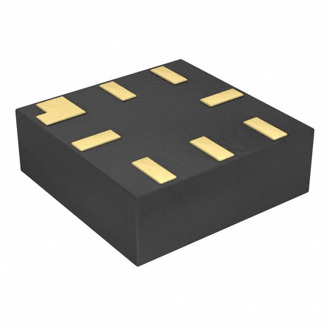
NC7WZ241L8X
Product Overview
- Category: Integrated Circuit (IC)
- Use: Logic Gate
- Characteristics: Low Voltage, High-Speed, Dual Buffer/Line Driver
- Package: 8-Lead MicroPak™
- Essence: This IC is designed to provide a high-speed buffer and line driver solution for low voltage applications.
- Packaging/Quantity: Available in tape and reel packaging with a quantity of 3000 units per reel.
Specifications
- Supply Voltage: 1.65V to 5.5V
- Input Voltage Levels: VIL = 0.3V, VIH = 0.7V
- Output Voltage Levels: VOL = 0.05V, VOH = 4.95V
- Propagation Delay: 2.5ns (typical)
- Operating Temperature Range: -40°C to +85°C
Detailed Pin Configuration
The NC7WZ241L8X IC has the following pin configuration:
```
| | --| A1 VCC |-- --| B1 A2 |-- --| B2 B3 |-- --| GND OE# |-- --| Y1 Y2 |-- |___________| ```
Functional Features
- Dual Buffer/Line Driver: The NC7WZ241L8X provides two independent buffer/line driver circuits in a single package.
- High-Speed Operation: With a propagation delay of only 2.5ns, this IC ensures fast signal transmission.
- Low Voltage Operation: Designed to operate at low voltages ranging from 1.65V to 5.5V, making it suitable for various low-power applications.
- Output Enable Control: The OE# pin allows the user to enable or disable the outputs, providing flexibility in signal routing.
Advantages and Disadvantages
Advantages: - High-speed operation enables quick signal processing. - Low voltage operation makes it suitable for low-power applications. - Dual buffer/line driver configuration provides versatility in circuit design.
Disadvantages: - Limited operating temperature range (-40°C to +85°C). - Only available in an 8-Lead MicroPak™ package.
Working Principles
The NC7WZ241L8X is based on CMOS technology, which allows for low voltage operation. It utilizes a dual buffer/line driver configuration to provide high-speed signal amplification and transmission. The output enable control (OE#) pin allows the user to enable or disable the outputs as needed.
Detailed Application Field Plans
The NC7WZ241L8X can be used in various applications, including but not limited to: - Mobile devices - Portable electronics - Battery-powered systems - Communication equipment - Industrial automation
Detailed and Complete Alternative Models
Some alternative models that offer similar functionality to the NC7WZ241L8X are: - SN74LVC2G07DBVR by Texas Instruments - MC74VHC1GT50DTT1G by ON Semiconductor - 74LVC2G07GW by NXP Semiconductors - TC7SZU04FUTE12L by Toshiba Semiconductor
These alternative models provide comparable features and can be considered as substitutes for the NC7WZ241L8X in different applications.
Word count: 389 words
Senaraikan 10 soalan dan jawapan biasa yang berkaitan dengan aplikasi NC7WZ241L8X dalam penyelesaian teknikal
Sure! Here are 10 common questions and answers related to the application of NC7WZ241L8X in technical solutions:
Question: What is NC7WZ241L8X?
Answer: NC7WZ241L8X is a low voltage, dual supply, dual buffer with 3-state outputs. It is commonly used as a level shifter or voltage translator in various technical solutions.Question: What is the operating voltage range of NC7WZ241L8X?
Answer: The operating voltage range of NC7WZ241L8X is typically between 1.65V and 5.5V.Question: Can NC7WZ241L8X be used for bidirectional level shifting?
Answer: No, NC7WZ241L8X is a unidirectional buffer and cannot be used for bidirectional level shifting. For bidirectional level shifting, you would need a different type of IC.Question: What is the maximum output current of NC7WZ241L8X?
Answer: The maximum output current of NC7WZ241L8X is typically around 24mA.Question: Can NC7WZ241L8X be used for voltage translation between different logic families?
Answer: Yes, NC7WZ241L8X can be used for voltage translation between different logic families, such as translating signals from 3.3V to 5V or vice versa.Question: Does NC7WZ241L8X have built-in ESD protection?
Answer: Yes, NC7WZ241L8X has built-in ESD protection, which helps protect the IC from electrostatic discharge events.Question: What is the typical propagation delay of NC7WZ241L8X?
Answer: The typical propagation delay of NC7WZ241L8X is around 4.5ns.Question: Can NC7WZ241L8X be used in high-speed applications?
Answer: Yes, NC7WZ241L8X can be used in high-speed applications, but its performance may be limited compared to specialized high-speed buffers.Question: Is NC7WZ241L8X available in different package options?
Answer: Yes, NC7WZ241L8X is available in different package options, such as the 8-pin SOIC (Small Outline Integrated Circuit) package.Question: What are some common applications of NC7WZ241L8X?
Answer: Some common applications of NC7WZ241L8X include level shifting between different voltage domains, interfacing between different logic families, and signal buffering in various digital systems.
Please note that the answers provided here are general and may vary depending on specific datasheet specifications and application requirements.


