

NL17SV32XV5T2
Basic Information Overview
- Category: Integrated Circuit (IC)
- Use: Logic Gate
- Characteristics: High-speed, Low-power consumption
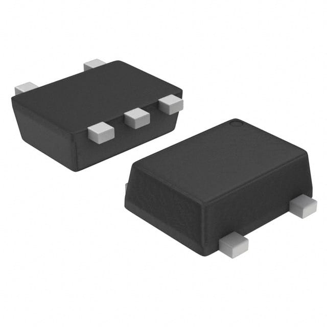
- Package: Small Outline Transistor (SOT) package
- Essence: Quad 2-input OR gate
- Packaging/Quantity: Tape and Reel, 3000 units per reel
Specifications
- Supply Voltage: 1.65V to 5.5V
- Input Voltage: -0.5V to VCC + 0.5V
- Output Voltage: -0.5V to VCC + 0.5V
- Operating Temperature Range: -40°C to +85°C
- Propagation Delay: 3.4ns (typical)
Detailed Pin Configuration
The NL17SV32XV5T2 has a total of 8 pins arranged as follows: 1. Pin 1: Input A 2. Pin 2: Input B 3. Pin 3: Ground (GND) 4. Pin 4: Output Y 5. Pin 5: VCC (Supply Voltage) 6. Pin 6: Input C 7. Pin 7: Input D 8. Pin 8: Not Connected (NC)
Functional Features
- Quad 2-input OR gate with Schmitt-trigger inputs
- High-speed operation for efficient logic processing
- Low-power consumption for energy-efficient applications
- Schmitt-trigger inputs provide hysteresis, improving noise immunity
Advantages and Disadvantages
Advantages: - High-speed operation enables quick data processing - Low-power consumption reduces energy usage and extends battery life - Schmitt-trigger inputs enhance noise immunity, ensuring reliable operation in noisy environments
Disadvantages: - Limited number of inputs (only 2 inputs per gate) - Not suitable for complex logic operations requiring multiple inputs
Working Principles
The NL17SV32XV5T2 is a quad 2-input OR gate that performs logical OR operations on two input signals. It utilizes Schmitt-trigger inputs, which provide hysteresis to improve noise immunity. When the input voltage exceeds a certain threshold, the output switches to a high state. Conversely, when the input voltage falls below another threshold, the output switches to a low state. This behavior ensures reliable operation even in the presence of noise or signal fluctuations.
Detailed Application Field Plans
The NL17SV32XV5T2 is commonly used in various digital systems and electronic devices where logical OR operations are required. Some application areas include: 1. Microcontrollers and microprocessors 2. Data communication systems 3. Industrial automation 4. Consumer electronics 5. Automotive electronics
Detailed and Complete Alternative Models
- SN74LVC32A: Quad 2-input OR gate with similar specifications and pin configuration.
- CD4071B: Quad 2-input OR gate with different package options and wider operating temperature range.
- MC14071B: Quad 2-input OR gate with higher supply voltage range and extended temperature range.
(Note: The above alternative models are just a few examples. There are several other alternatives available in the market.)
This entry provides an overview of the NL17SV32XV5T2 integrated circuit, including its basic information, specifications, pin configuration, functional features, advantages and disadvantages, working principles, application field plans, and alternative models. With its high-speed operation, low-power consumption, and Schmitt-trigger inputs, this logic gate offers reliable performance in various digital systems and electronic devices.
Senaraikan 10 soalan dan jawapan biasa yang berkaitan dengan aplikasi NL17SV32XV5T2 dalam penyelesaian teknikal
Sure! Here are 10 common questions and answers related to the application of NL17SV32XV5T2 in technical solutions:
Q: What is NL17SV32XV5T2? A: NL17SV32XV5T2 is a specific model of integrated circuit (IC) or chip used in electronic devices.
Q: What is the purpose of NL17SV32XV5T2? A: NL17SV32XV5T2 is commonly used as a voltage level translator, converting signals between different voltage levels in electronic circuits.
Q: What voltage levels can NL17SV32XV5T2 handle? A: NL17SV32XV5T2 can handle voltage levels ranging from 1.2V to 3.6V.
Q: How many channels does NL17SV32XV5T2 have? A: NL17SV32XV5T2 has 4 channels, allowing it to translate signals between multiple input and output pins.
Q: Can NL17SV32XV5T2 be used bidirectionally? A: Yes, NL17SV32XV5T2 supports bidirectional signal translation, allowing signals to be translated in both directions.
Q: What is the maximum data rate supported by NL17SV32XV5T2? A: NL17SV32XV5T2 can support data rates up to 100 Mbps.
Q: Is NL17SV32XV5T2 compatible with different logic families? A: Yes, NL17SV32XV5T2 is compatible with various logic families such as CMOS, TTL, and LVCMOS.
Q: Can NL17SV32XV5T2 be used in battery-powered devices? A: Yes, NL17SV32XV5T2 is designed to operate efficiently in low-power applications, making it suitable for battery-powered devices.
Q: Are there any specific precautions when using NL17SV32XV5T2? A: It is important to ensure that the voltage levels and signal timings are within the specified limits mentioned in the datasheet of NL17SV32XV5T2.
Q: Where can I find more information about NL17SV32XV5T2? A: You can refer to the datasheet provided by the manufacturer or visit their official website for detailed information on NL17SV32XV5T2's specifications and application notes.
Please note that the answers provided here are general and may vary depending on the specific requirements and use cases.