

NSVMMUN2112LT1G
Product Overview
- Category: Semiconductor
- Use: Power transistor for electronic circuits
- Characteristics: High voltage, low power consumption, compact size
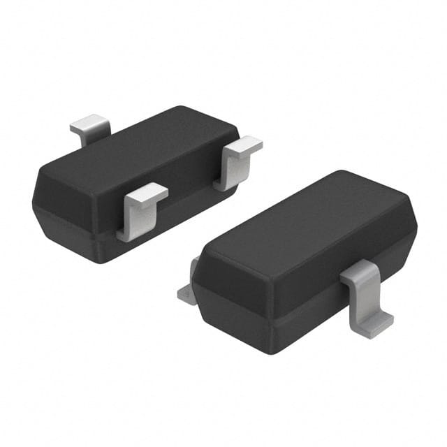
- Package: SOT-23
- Essence: NPN bipolar junction transistor
- Packaging/Quantity: Tape and reel, 3000 units per reel
Specifications
- Voltage Rating: 50V
- Current Rating: 200mA
- Power Dissipation: 225mW
- Transition Frequency: 250MHz
- Operating Temperature Range: -55°C to 150°C
Detailed Pin Configuration
- Base (B)
- Emitter (E)
- Collector (C)
Functional Features
- High voltage capability
- Low leakage current
- Fast switching speed
- Small footprint
Advantages and Disadvantages
Advantages
- Suitable for high voltage applications
- Low power consumption
- Compact size
Disadvantages
- Limited current handling capacity
- Sensitive to overvoltage conditions
Working Principles
The NSVMMUN2112LT1G operates based on the principles of bipolar junction transistors, utilizing the flow of charge carriers to control current. When a small current is applied to the base terminal, it controls the larger current flowing between the collector and emitter terminals.
Detailed Application Field Plans
The NSVMMUN2112LT1G is commonly used in low-power electronic circuits such as amplifiers, signal processing, and voltage regulation. Its high voltage capability makes it suitable for applications requiring voltage amplification and switching.
Detailed and Complete Alternative Models
- BC547: Similar NPN transistor with lower voltage rating
- 2N3904: General-purpose NPN transistor with comparable characteristics
- MMBT2222A: SMD NPN transistor with similar package and characteristics
Note: The alternative models listed above are provided for reference and may require adjustments based on specific application requirements.
This comprehensive entry provides an in-depth understanding of the NSVMMUN2112LT1G, covering its specifications, functional features, advantages, disadvantages, working principles, application field plans, and alternative models.
Senaraikan 10 soalan dan jawapan biasa yang berkaitan dengan aplikasi NSVMMUN2112LT1G dalam penyelesaian teknikal
Sure, here are 10 common questions and answers related to the application of NSVMMUN2112LT1G in technical solutions:
What is NSVMMUN2112LT1G?
- NSVMMUN2112LT1G is a voltage regulator designed for use in various technical solutions to provide stable and regulated voltage output.
What is the input voltage range for NSVMMUN2112LT1G?
- The input voltage range for NSVMMUN2112LT1G is typically between 4.5V to 18V.
What is the output voltage range for NSVMMUN2112LT1G?
- The output voltage range for NSVMMUN2112LT1G is typically between 1.2V to 16V.
What is the maximum output current of NSVMMUN2112LT1G?
- The maximum output current of NSVMMUN2112LT1G is typically around 1A.
What are the typical applications of NSVMMUN2112LT1G?
- NSVMMUN2112LT1G is commonly used in applications such as power supplies, battery-powered devices, and other electronic systems requiring voltage regulation.
Does NSVMMUN2112LT1G have built-in protection features?
- Yes, NSVMMUN2112LT1G typically includes overcurrent protection, thermal shutdown, and reverse polarity protection.
Is NSVMMUN2112LT1G suitable for automotive applications?
- Yes, NSVMMUN2112LT1G is often suitable for automotive applications due to its wide input voltage range and robust design.
What is the operating temperature range for NSVMMUN2112LT1G?
- The operating temperature range for NSVMMUN2112LT1G is typically between -40°C to 125°C.
Can NSVMMUN2112LT1G be used in conjunction with other voltage regulators?
- Yes, NSVMMUN2112LT1G can be used in parallel or in combination with other voltage regulators to achieve higher output currents or specific performance requirements.
Are there any specific layout considerations for using NSVMMUN2112LT1G in a PCB design?
- Yes, it's important to follow the manufacturer's recommended layout guidelines to minimize noise, optimize thermal performance, and ensure stability when using NSVMMUN2112LT1G in a PCB design.