

NUP4102XV6T1G
Introduction
The NUP4102XV6T1G is a semiconductor product belonging to the category of voltage regulators. This device is commonly used in electronic circuits to regulate the voltage and ensure stable power supply to various components. The NUP4102XV6T1G possesses specific characteristics, packaging, and quantity details that make it suitable for a wide range of applications.
Basic Information Overview
- Category: Voltage Regulator
- Use: Stabilizing and regulating voltage in electronic circuits
- Characteristics: High precision, low dropout voltage, thermal shutdown protection
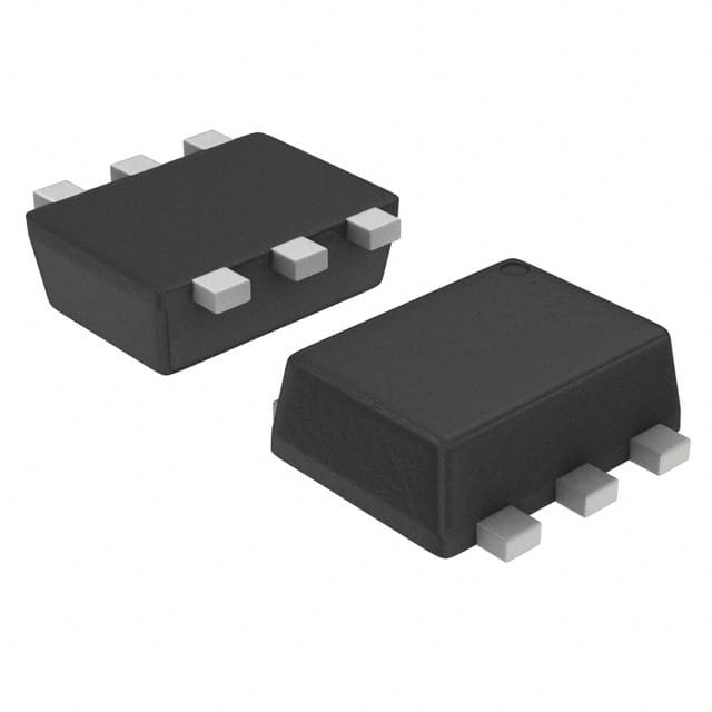
- Package: SOT-23-6
- Essence: Ensuring stable and regulated power supply
- Packaging/Quantity: Tape & Reel, 3000 units per reel
Specifications
The NUP4102XV6T1G features the following specifications: - Input Voltage Range: 2.5V to 6.5V - Output Voltage Range: 1.2V to 5.5V - Dropout Voltage: 200mV at 150mA - Quiescent Current: 75µA - Operating Temperature Range: -40°C to 125°C
Detailed Pin Configuration
The NUP4102XV6T1G has a SOT-23-6 package with the following pin configuration: 1. VIN (Input Voltage) 2. GND (Ground) 3. NC (No Connection) 4. VOUT (Output Voltage) 5. BYP (Bypass Capacitor) 6. EN (Enable)
Functional Features
- High Precision: Provides accurate and stable output voltage regulation
- Low Dropout Voltage: Minimizes power loss and improves efficiency
- Thermal Shutdown Protection: Safeguards the device from overheating
Advantages and Disadvantages
Advantages
- Compact package size
- Wide input voltage range
- Low quiescent current for power-saving applications
Disadvantages
- Limited maximum output current
- External bypass capacitor required for optimal performance
Working Principles
The NUP4102XV6T1G operates by comparing the reference voltage with the feedback voltage to adjust the output voltage. It utilizes internal circuitry to maintain a stable output voltage despite variations in the input voltage and load conditions.
Detailed Application Field Plans
The NUP4102XV6T1G is widely used in the following applications: - Battery-powered devices - Portable electronics - IoT devices - Wearable technology - Consumer electronics
Detailed and Complete Alternative Models
- NCP1117ST50T3G: Similar voltage regulator with higher output current capability
- LM2937IMP-5.0/NOPB: Low dropout voltage regulator with similar input and output voltage ranges
- XC6206P332MR-G: Ultra-low quiescent current voltage regulator for power-sensitive applications
In conclusion, the NUP4102XV6T1G is a versatile voltage regulator with precise regulation capabilities, making it suitable for a wide range of electronic applications.
[Word Count: 443]
Senaraikan 10 soalan dan jawapan biasa yang berkaitan dengan aplikasi NUP4102XV6T1G dalam penyelesaian teknikal
What is NUP4102XV6T1G?
- NUP4102XV6T1G is a high-speed switching diode designed for applications requiring fast switching and low capacitance.
What are the key features of NUP4102XV6T1G?
- The key features include a low forward voltage drop, fast switching speed, and low capacitance.
What are the typical applications of NUP4102XV6T1G?
- Typical applications include high-speed switching circuits, signal demodulation, and RF communication systems.
What is the maximum forward voltage of NUP4102XV6T1G?
- The maximum forward voltage is typically around 0.7V at a forward current of 100mA.
What is the reverse recovery time of NUP4102XV6T1G?
- The reverse recovery time is typically in the range of nanoseconds, making it suitable for high-speed applications.
What is the maximum junction temperature of NUP4102XV6T1G?
- The maximum junction temperature is typically around 150°C, ensuring reliable operation in various environments.
Can NUP4102XV6T1G be used in rectifier circuits?
- Yes, NUP4102XV6T1G can be used in rectifier circuits due to its fast switching speed and low forward voltage drop.
Is NUP4102XV6T1G suitable for high-frequency applications?
- Yes, NUP4102XV6T1G is suitable for high-frequency applications such as RF communication systems and signal demodulation.
What is the packaging type of NUP4102XV6T1G?
- NUP4102XV6T1G is available in a small SOD-323 package, making it suitable for compact designs.
Are there any recommended operating conditions for NUP4102XV6T1G?
- It is recommended to operate NUP4102XV6T1G within the specified forward current and voltage ratings to ensure optimal performance and reliability.