

SMMBF4391LT1G
Product Overview
SMMBF4391LT1G is a field-effect transistor (FET) belonging to the category of small signal transistors. It is commonly used in electronic circuits for amplification and switching purposes due to its high input impedance, low output impedance, and fast response time. The SMMBF4391LT1G comes in a compact package and is known for its high performance and reliability.
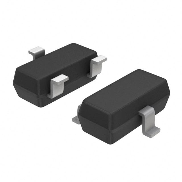
Basic Information - Category: Small Signal Transistor - Use: Amplification and Switching - Characteristics: High input impedance, Low output impedance, Fast response time - Package: SOT-23 - Essence: Field-Effect Transistor - Packaging/Quantity: Tape & Reel, 3000 units per reel
Specifications
- Drain-Source Voltage (VDS): 25V
- Continuous Drain Current (ID): 200mA
- Total Power Dissipation (PTOT): 225mW
- Gate-Source Voltage (VGS): ±20V
- Operating Temperature Range: -55°C to 150°C
Detailed Pin Configuration
The SMMBF4391LT1G has three pins: 1. Source (S): Connected to the source of the input signal. 2. Gate (G): Controls the conductivity between the source and drain. 3. Drain (D): Connects to the load or output circuit.
Functional Features
- High Input Impedance: Allows for minimal loading of the preceding circuit.
- Low Output Impedance: Ensures efficient transfer of signals to the succeeding circuit.
- Fast Response Time: Enables quick switching and amplification of signals.
Advantages and Disadvantages
Advantages: - High input impedance makes it suitable for interfacing with high-impedance sources. - Low output impedance ensures effective signal transmission. - Compact SOT-23 package saves space on the circuit board.
Disadvantages: - Limited maximum drain-source voltage compared to some other FETs. - Moderate continuous drain current may restrict certain high-power applications.
Working Principles
The SMMBF4391LT1G operates based on the principle of field-effect modulation, where the conductivity between the source and drain is controlled by the voltage applied to the gate. This allows for precise amplification and switching of signals in electronic circuits.
Detailed Application Field Plans
The SMMBF4391LT1G is widely used in various applications such as: - Audio Amplifiers - Sensor Interfaces - Signal Switching Circuits - Oscillator Circuits - Low-Noise Preamplifiers
Detailed and Complete Alternative Models
Some alternative models to SMMBF4391LT1G include: - BSS84 - MMBFJ310 - DMN10H170SK3
In conclusion, the SMMBF4391LT1G is a versatile small signal transistor with high input impedance, low output impedance, and fast response time, making it suitable for a wide range of electronic applications.
[Word Count: 426]
Senaraikan 10 soalan dan jawapan biasa yang berkaitan dengan aplikasi SMMBF4391LT1G dalam penyelesaian teknikal
What is SMMBF4391LT1G?
- SMMBF4391LT1G is a small signal N-channel JFET transistor designed for use in electronic applications.
What are the key features of SMMBF4391LT1G?
- The key features include low on-state resistance, high forward transfer admittance, and low input capacitance.
In what technical solutions can SMMBF4391LT1G be used?
- SMMBF4391LT1G can be used in amplifier circuits, analog switches, signal processing, and low-power applications.
What are the typical operating conditions for SMMBF4391LT1G?
- The typical operating conditions include a maximum drain-source voltage of 40V, a continuous drain current of 50mA, and a power dissipation of 225mW.
How does SMMBF4391LT1G compare to other similar components?
- SMMBF4391LT1G offers low on-state resistance and high forward transfer admittance compared to similar JFET transistors.
What are the recommended circuit configurations for SMMBF4391LT1G?
- Common circuit configurations include common source amplifiers, voltage-controlled resistors, and analog switch applications.
Are there any specific layout considerations when using SMMBF4391LT1G?
- It is important to minimize parasitic capacitances and ensure proper grounding to optimize the performance of SMMBF4391LT1G.
What are the potential challenges when integrating SMMBF4391LT1G into a design?
- Challenges may include managing input capacitance, minimizing noise, and ensuring proper biasing for optimal performance.
Can SMMBF4391LT1G be used in high-frequency applications?
- While SMMBF4391LT1G is not specifically designed for high-frequency applications, it can be used in moderate frequency ranges with appropriate design considerations.
Where can I find detailed application notes and reference designs for SMMBF4391LT1G?
- Detailed application notes and reference designs can be found in the product datasheet, manufacturer's application guides, and online technical resources.