
DTC143TMT2L
Introduction
The DTC143TMT2L is a versatile transistor that belongs to the category of discrete semiconductor products. This entry provides an overview of the basic information, specifications, detailed pin configuration, functional features, advantages and disadvantages, working principles, detailed application field plans, and alternative models of the DTC143TMT2L.
Basic Information Overview
- Category: Discrete Semiconductor Product
- Use: The DTC143TMT2L is commonly used as a switching device in electronic circuits.
- Characteristics: It exhibits high voltage capability and low saturation voltage, making it suitable for various applications.
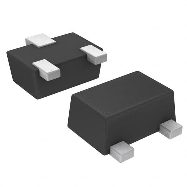
- Package: SOT-23
- Essence: The essence of the DTC143TMT2L lies in its ability to efficiently control the flow of current in electronic circuits.
- Packaging/Quantity: Typically available in reels with varying quantities based on manufacturer specifications.
Specifications
- Type: PNP
- Maximum Collector-Base Voltage (VCBO): -50V
- Maximum Collector-Emitter Voltage (VCEO): -50V
- Maximum Emitter-Base Voltage (VEBO): -5V
- Continuous Collector Current (IC): -100mA
- Power Dissipation (PD): 200mW
- Transition Frequency (ft): 150MHz
- Operating Temperature Range: -55°C to +150°C
Detailed Pin Configuration
The DTC143TMT2L has three pins: Collector (C), Base (B), and Emitter (E). The pin configuration is as follows: - Collector (C): Pin 1 - Base (B): Pin 2 - Emitter (E): Pin 3
Functional Features
- High Voltage Capability: The DTC143TMT2L can withstand relatively high voltages, making it suitable for diverse circuit designs.
- Low Saturation Voltage: This feature ensures minimal power loss during operation, contributing to energy-efficient designs.
- Fast Switching Speed: The transistor offers rapid switching capabilities, enabling quick response in electronic circuits.
Advantages and Disadvantages
Advantages
- Versatile application in various electronic circuits
- Low saturation voltage leads to improved energy efficiency
- Compact SOT-23 package allows for space-efficient designs
Disadvantages
- Limited maximum collector current compared to some alternative models
- Operating temperature range may not be suitable for extreme environments
Working Principles
The DTC143TMT2L operates based on the principles of PNP transistor behavior. When a small current flows into the base terminal, it controls a larger current between the collector and emitter terminals, allowing for signal amplification or switching functions within electronic circuits.
Detailed Application Field Plans
The DTC143TMT2L finds extensive use in the following application fields: - Switching Circuits: It is employed in various electronic switches due to its fast switching speed and low saturation voltage. - Amplification Circuits: The transistor is utilized in signal amplification applications where controlled current flow is essential. - Voltage Regulation: Its high voltage capability makes it suitable for voltage regulation tasks in electronic systems.
Detailed and Complete Alternative Models
- DTC143ZETL: Similar characteristics with enhanced power dissipation capabilities
- DTC144TETL: Higher maximum collector current with comparable voltage ratings
- DTC123JETL: Lower saturation voltage and faster switching speed for specific applications
In conclusion, the DTC143TMT2L is a valuable component in electronic circuit design, offering a balance of performance and efficiency. Its specifications, functional features, and application versatility make it a popular choice for various electronic applications.
[Word Count: 533]
Senaraikan 10 soalan dan jawapan biasa yang berkaitan dengan aplikasi DTC143TMT2L dalam penyelesaian teknikal
What is the DTC143TMT2L transistor used for?
- The DTC143TMT2L is a general-purpose NPN digital transistor used for switching and amplification in various technical solutions.
What are the key specifications of the DTC143TMT2L transistor?
- The DTC143TMT2L has a maximum collector current of 100mA, a maximum collector-emitter voltage of 50V, and a maximum power dissipation of 150mW.
How can I use the DTC143TMT2L in a switching application?
- The DTC143TMT2L can be used as a switch by connecting the base to the control signal and using the collector-emitter path to control the load.
Can the DTC143TMT2L be used in amplifier circuits?
- Yes, the DTC143TMT2L can be used in low-power amplifier circuits due to its NPN configuration and moderate current and voltage ratings.
What are some typical applications of the DTC143TMT2L in technical solutions?
- The DTC143TMT2L is commonly used in logic level shifting, level translation, signal inversion, and general purpose switching applications.
Are there any specific considerations for driving inductive loads with the DTC143TMT2L?
- When driving inductive loads, it's important to include a flyback diode across the load to protect the transistor from voltage spikes.
What is the pinout configuration of the DTC143TMT2L transistor?
- The DTC143TMT2L typically has the emitter connected to the ground, the collector as the output, and the base as the input control terminal.
Can the DTC143TMT2L be used in high-frequency applications?
- The DTC143TMT2L is not designed for high-frequency applications due to its moderate speed characteristics.
What are the temperature limitations of the DTC143TMT2L?
- The DTC143TMT2L has an operating temperature range of -55°C to 150°C, making it suitable for a wide range of environments.
Are there any recommended alternative transistors to the DTC143TMT2L?
- Some alternative transistors with similar characteristics include 2N3904, BC547, and PN2222A. Always refer to the datasheets for specific comparisons and compatibility.