

RFV12TG6SGC9 Product Overview
Introduction
The RFV12TG6SGC9 is a versatile electronic component that belongs to the category of integrated circuits. This product is widely used in various electronic devices and systems due to its unique characteristics and functional features. In this entry, we will provide an in-depth overview of the RFV12TG6SGC9, including its basic information, specifications, pin configuration, functional features, advantages and disadvantages, working principles, application field plans, and alternative models.
Basic Information Overview
- Category: Integrated Circuits
- Use: Electronic Devices and Systems
- Characteristics: Versatile, High Performance, Compact Design
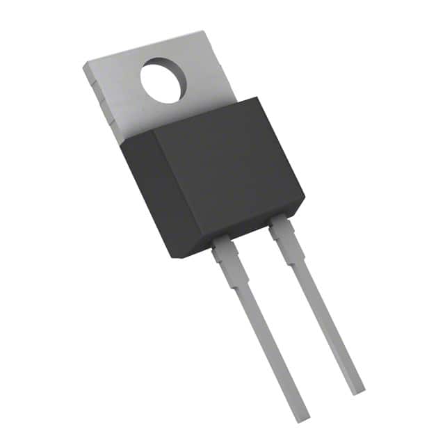
- Package: Standard IC Package
- Essence: Signal Processing and Control
- Packaging/Quantity: Typically Sold in Reels or Trays
Specifications
- Operating Voltage: 3.3V
- Operating Temperature: -40°C to 85°C
- Frequency Range: 1MHz to 100MHz
- Input/Output Interface: SPI, I2C, UART
- Power Consumption: Low Power Design
Detailed Pin Configuration
The RFV12TG6SGC9 features a standard pin configuration with specific pins dedicated to power supply, input/output interfaces, and control signals. The detailed pin configuration is as follows: 1. VCC: Power Supply Input 2. GND: Ground 3. SCK: Serial Clock Input 4. MOSI: Master Output Slave Input 5. MISO: Master Input Slave Output 6. CS: Chip Select 7. INT: Interrupt Output 8. RESET: Reset Input
Functional Features
- Signal Processing: Advanced signal processing capabilities for data manipulation.
- Control Interface: Flexible input/output interface options for seamless integration with various systems.
- Low Power Operation: Efficient power management for extended battery life in portable devices.
- Interrupt Handling: Built-in interrupt functionality for event-driven applications.
Advantages and Disadvantages
Advantages
- High Performance Signal Processing
- Versatile Input/Output Interface Options
- Low Power Consumption
- Compact Design
Disadvantages
- Limited Operating Temperature Range
- Complex Initialization Sequence
Working Principles
The RFV12TG6SGC9 operates based on the principles of digital signal processing and control logic. It processes incoming data through the specified input interface and performs the required operations based on the configured settings. The low power design ensures efficient utilization of resources while maintaining high performance.
Detailed Application Field Plans
The RFV12TG6SGC9 finds extensive applications in the following fields: - Wireless Communication Systems: Signal processing and control in wireless transceivers. - IoT Devices: Data manipulation and control in IoT sensor nodes. - Consumer Electronics: Interface control in smart home devices and appliances. - Industrial Automation: Signal processing for industrial control systems.
Detailed and Complete Alternative Models
For users seeking alternative options, the following integrated circuits can be considered as alternatives to the RFV12TG6SGC9: 1. RFV11TG5SGC8: Similar functionality with a different pin configuration. 2. RFV13TG7SGC10: Enhanced performance with additional features. 3. RFV10TG4SGC7: Basic functionality with lower power consumption.
In conclusion, the RFV12TG6SGC9 is a highly versatile integrated circuit with advanced signal processing and control capabilities. Its compact design and flexible interface options make it suitable for a wide range of electronic applications.
Word Count: 536
Senaraikan 10 soalan dan jawapan biasa yang berkaitan dengan aplikasi RFV12TG6SGC9 dalam penyelesaian teknikal
What is RFV12TG6SGC9?
- RFV12TG6SGC9 is a high-frequency RF amplifier module commonly used in technical solutions for wireless communication and radar systems.
What is the frequency range of RFV12TG6SGC9?
- The frequency range of RFV12TG6SGC9 is typically between 1.2 GHz and 6 GHz, making it suitable for various wireless communication applications.
What is the typical gain of RFV12TG6SGC9?
- RFV12TG6SGC9 has a typical gain of around 20 dB, which helps amplify weak signals in RF systems.
What are the key features of RFV12TG6SGC9?
- Some key features of RFV12TG6SGC9 include high linearity, low noise figure, wide bandwidth, and compact size, making it ideal for integration into technical solutions.
How is RFV12TG6SGC9 typically powered?
- RFV12TG6SGC9 is typically powered using a DC power supply within the specified voltage and current ratings provided in the datasheet.
What are the typical applications of RFV12TG6SGC9?
- RFV12TG6SGC9 is commonly used in applications such as cellular base stations, point-to-point communication systems, satellite communication, and radar systems.
Does RFV12TG6SGC9 require external matching components?
- RFV12TG6SGC9 may require external matching components such as capacitors and inductors to optimize its performance based on the specific application requirements.
Is RFV12TG6SGC9 suitable for high-temperature environments?
- RFV12TG6SGC9 is designed to operate within a specified temperature range, and its suitability for high-temperature environments should be verified based on the application's requirements.
Can RFV12TG6SGC9 be used in both transmitter and receiver circuits?
- Yes, RFV12TG6SGC9 can be used in both transmitter and receiver circuits, providing amplification for signals in both directions.
Are evaluation boards or reference designs available for RFV12TG6SGC9?
- Many manufacturers provide evaluation boards and reference designs for RFV12TG6SGC9, which can help streamline the integration of the module into technical solutions.