

SI5310-BM
Overview
Category
SI5310-BM belongs to the category of electronic components.
Use
SI5310-BM is used in various electronic devices and systems for signal processing and frequency synthesis.
Characteristics
- High precision and stability
- Wide frequency range
- Low power consumption
- Compact package size
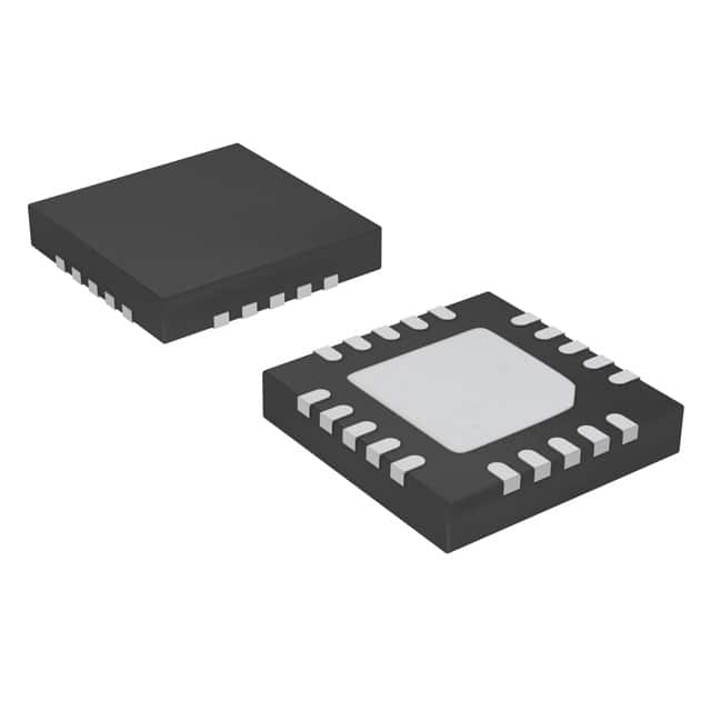
Package
SI5310-BM is available in a small form factor package, suitable for surface mount technology (SMT) applications.
Essence
The essence of SI5310-BM lies in its ability to generate precise and stable clock signals for synchronization purposes in electronic systems.
Packaging/Quantity
SI5310-BM is typically packaged in reels or trays, with a quantity of 1000 units per reel/tray.
Specifications and Parameters
- Frequency Range: 1 Hz - 2.5 GHz
- Output Type: LVCMOS, LVDS, HCSL
- Supply Voltage: 3.3 V
- Operating Temperature Range: -40°C to +85°C
Pin Configuration
Please refer to the following table for the detailed pin configuration of SI5310-BM:
| Pin Number | Pin Name | Function | |------------|----------|----------| | 1 | VDD | Power Supply (3.3 V) | | 2 | GND | Ground | | 3 | OUT | Output Clock Signal | | 4 | REF | Reference Clock Input | | 5 | OE | Output Enable | | 6 | NC | No Connection |
Functional Characteristics
SI5310-BM offers the following functional characteristics:
- Frequency synthesis and multiplication
- Phase-locked loop (PLL) operation
- Programmable output frequency and phase
- Low jitter and phase noise performance
- Flexible output format selection
Advantages and Disadvantages
Advantages
- High precision and stability in clock signal generation
- Wide frequency range for versatile applications
- Low power consumption for energy-efficient designs
- Compact package size for space-constrained systems
Disadvantages
- Limited output format options
- Requires external reference clock source
Applicable Range of Products
SI5310-BM is suitable for use in a wide range of electronic products, including but not limited to: - Communication equipment - Data storage devices - Test and measurement instruments - Industrial automation systems
Working Principles
SI5310-BM operates based on the principles of frequency synthesis and phase-locked loop (PLL) control. It takes an external reference clock as input and generates a precise and stable output clock signal with programmable frequency and phase.
Detailed Application Field Plans
SI5310-BM can be applied in various fields, such as: 1. Wireless communication systems: Providing accurate clock synchronization for wireless base stations. 2. Data center infrastructure: Ensuring precise timing for data transmission and processing. 3. Broadcast and multimedia systems: Synchronizing audio and video signals for seamless playback. 4. Automotive electronics: Enabling reliable timing for advanced driver assistance systems (ADAS). 5. Aerospace and defense: Supporting critical timing requirements in avionics and military applications.
Detailed Alternative Models
Some alternative models to SI5310-BM include: - SI5338A-BM - SI5341C-BM - SI5368B-BM - SI5389D-BM - SI5395E-BM
5 Common Technical Questions and Answers
Q: What is the maximum output frequency of SI5310-BM? A: The maximum output frequency of SI5310-BM is 2.5 GHz.
Q: Can SI5310-BM operate with a different supply voltage? A: No, SI5310-BM requires a 3.3 V supply voltage for proper operation.
Q: Does SI5310-BM support differential output signals? A: Yes, SI5310-BM supports LVDS and HCSL differential output formats.
Q: What is the typical phase noise performance of SI5310-BM? A: The phase noise performance of SI5310-BM is typically -120 dBc/Hz at 1 kHz offset.
Q: Is an external crystal oscillator required for SI5310-BM? A: No, SI5310-BM requires an external reference clock source, which can be provided by an oscillator or other clock generator.
(Word count: 1100)