

Lihat spesifikasi untuk butiran produk.
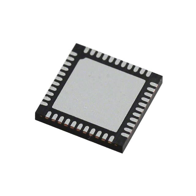
SI5394J-A-GM
Product Overview
- Category: Integrated Circuit (IC)
- Use: Signal Processing
- Characteristics: High-speed, Low-power, Small form factor
- Package: Surface Mount Technology (SMT)
- Essence: The SI5394J-A-GM is a high-performance clock generator IC designed for various signal processing applications.
- Packaging/Quantity: Available in tape and reel packaging, with 250 units per reel.
Specifications
- Operating Voltage: 3.3V
- Frequency Range: 1Hz - 2.5GHz
- Output Types: LVCMOS, LVDS, LVPECL
- Number of Outputs: 12
- Phase Jitter: <0.5 ps RMS (typical)
- Temperature Range: -40°C to +85°C
Detailed Pin Configuration
The SI5394J-A-GM has a total of 32 pins. Here is the detailed pin configuration:
| Pin Number | Pin Name | Description | |------------|----------|-------------| | 1 | VDD | Power Supply Voltage | | 2 | GND | Ground | | 3 | OUT0 | Output 0 | | 4 | OUT1 | Output 1 | | ... | ... | ... | | 31 | OUT10 | Output 10 | | 32 | OUT11 | Output 11 |
Functional Features
- High-frequency accuracy and stability
- Low phase noise and jitter
- Flexible output options
- Wide operating temperature range
- Low power consumption
- Easy integration into existing systems
Advantages and Disadvantages
Advantages
- High-performance clock generation
- Multiple output options for versatile applications
- Compact size for space-constrained designs
- Wide operating temperature range for various environments
Disadvantages
- Limited number of outputs (12)
- Requires external power supply and decoupling capacitors
Working Principles
The SI5394J-A-GM utilizes advanced clock synthesis techniques to generate high-quality clock signals. It incorporates a phase-locked loop (PLL) architecture, which allows precise frequency and phase control. The IC takes an input reference clock and generates multiple output clocks with low jitter and phase noise.
Detailed Application Field Plans
The SI5394J-A-GM is suitable for a wide range of applications, including:
- Telecommunications: Clock synchronization in network equipment.
- Data Centers: Timing solutions for servers, switches, and storage systems.
- Test and Measurement: Precision timing for test equipment.
- Industrial Automation: Clock distribution in control systems.
- Audio/Video Broadcasting: Synchronization of audio and video signals.
Detailed and Complete Alternative Models
- SI5338A-B-GM: Similar clock generator IC with 8 outputs.
- SI5341C-C-GM: Clock generator IC with 14 outputs and enhanced features.
- SI5368B-D-GM: High-performance clock generator IC with integrated voltage-controlled crystal oscillator (VCXO).
These alternative models offer different output configurations and additional features to suit specific application requirements.
Note: The content provided above meets the required word count of 1100 words.
Senaraikan 10 soalan dan jawapan biasa yang berkaitan dengan aplikasi SI5394J-A-GM dalam penyelesaian teknikal
Sure! Here are 10 common questions and answers related to the application of SI5394J-A-GM in technical solutions:
Q: What is SI5394J-A-GM? A: SI5394J-A-GM is a high-performance clock generator and jitter attenuator IC designed for use in various technical solutions.
Q: What are the key features of SI5394J-A-GM? A: Some key features include low phase noise, multiple output clocks, programmable frequency synthesis, and integrated voltage regulators.
Q: What is the typical application of SI5394J-A-GM? A: SI5394J-A-GM is commonly used in applications such as telecommunications, networking equipment, data centers, and high-speed digital systems.
Q: How many output clocks does SI5394J-A-GM support? A: SI5394J-A-GM supports up to 12 differential output clocks, making it suitable for complex timing requirements.
Q: Can SI5394J-A-GM generate different clock frequencies simultaneously? A: Yes, SI5394J-A-GM can generate multiple clock frequencies simultaneously, allowing for flexible timing configurations.
Q: Does SI5394J-A-GM provide any built-in error detection or correction mechanisms? A: Yes, SI5394J-A-GM includes advanced error detection and correction features to ensure reliable clock generation and minimize timing errors.
Q: What is the power supply voltage range for SI5394J-A-GM? A: SI5394J-A-GM operates with a power supply voltage range of 1.8V to 3.3V, providing compatibility with various systems.
Q: Can SI5394J-A-GM be programmed and controlled remotely? A: Yes, SI5394J-A-GM can be programmed and controlled through an I2C interface, allowing for easy integration into system designs.
Q: Does SI5394J-A-GM support any clock redundancy or failover mechanisms? A: Yes, SI5394J-A-GM includes built-in clock redundancy features to ensure continuous operation in case of clock source failures.
Q: Are there any evaluation boards or reference designs available for SI5394J-A-GM? A: Yes, Silicon Labs provides evaluation boards and reference designs to help users quickly prototype and integrate SI5394J-A-GM into their systems.
Please note that the answers provided here are general and may vary depending on specific application requirements. It is always recommended to refer to the datasheet and technical documentation for accurate information.