

Encyclopedia Entry: 74ALVC16834DGVRG4
Product Overview
Category
The 74ALVC16834DGVRG4 belongs to the category of integrated circuits (ICs).
Use
This IC is commonly used in digital electronic systems for signal transmission and processing.
Characteristics
- Low voltage operation
- High-speed performance
- Wide operating temperature range
- Low power consumption
Package
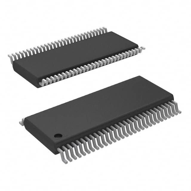
The 74ALVC16834DGVRG4 is available in a small form factor package, such as a VSSOP (Very Small Outline Package).
Essence
The essence of this product lies in its ability to provide efficient and reliable signal transmission and processing in digital electronic systems.
Packaging/Quantity
The 74ALVC16834DGVRG4 is typically packaged in reels or tubes, with a quantity of around 2500 units per reel/tube.
Specifications
- Supply Voltage: 1.2V - 3.6V
- Operating Temperature Range: -40°C to +85°C
- Input/Output Compatibility: LVTTL/TTL
- Number of Channels: 8
- Logic Family: ALVC
- Output Drive Capability: ±24mA
Detailed Pin Configuration
The 74ALVC16834DGVRG4 has a total of 48 pins, which are organized as follows:
- Pin 1: GND (Ground)
- Pin 2: A1 (Input/Output)
- Pin 3: Y1 (Output)
- Pin 4: A2 (Input/Output)
- Pin 5: Y2 (Output)
- Pin 6: A3 (Input/Output)
- Pin 7: Y3 (Output)
- Pin 8: A4 (Input/Output)
- Pin 9: Y4 (Output)
- Pin 10: A5 (Input/Output)
- Pin 11: Y5 (Output)
- Pin 12: A6 (Input/Output)
- Pin 13: Y6 (Output)
- Pin 14: A7 (Input/Output)
- Pin 15: Y7 (Output)
- Pin 16: A8 (Input/Output)
- Pin 17: Y8 (Output)
- Pin 18: GND (Ground)
- Pin 19: B1 (Input/Output)
- Pin 20: Z1 (Output)
- Pin 21: B2 (Input/Output)
- Pin 22: Z2 (Output)
- Pin 23: B3 (Input/Output)
- Pin 24: Z3 (Output)
- Pin 25: B4 (Input/Output)
- Pin 26: Z4 (Output)
- Pin 27: B5 (Input/Output)
- Pin 28: Z5 (Output)
- Pin 29: B6 (Input/Output)
- Pin 30: Z6 (Output)
- Pin 31: B7 (Input/Output)
- Pin 32: Z7 (Output)
- Pin 33: B8 (Input/Output)
- Pin 34: Z8 (Output)
- Pin 35: VCC (Power Supply)
- Pin 36: OE (Output Enable)
- Pin 37: G1 (Enable Input)
- Pin 38: G2 (Enable Input)
- Pin 39: G3 (Enable Input)
- Pin 40: G4 (Enable Input)
- Pin 41: G5 (Enable Input)
- Pin 42: G6 (Enable Input)
- Pin 43: G7 (Enable Input)
- Pin 44: G8 (Enable Input)
- Pin 45: GND (Ground)
- Pin 46: NC (No Connection)
- Pin 47: NC (No Connection)
- Pin 48: VCC (Power Supply)
Functional Features
- High-speed signal transmission and processing
- Low power consumption
- Wide operating temperature range
- Compatibility with LVTTL/TTL logic levels
- Output drive capability of ±24mA
Advantages and Disadvantages
Advantages
- Efficient signal transmission and processing
- Low power consumption
- Compact form factor
- Wide operating temperature range
Disadvantages
- Limited number of channels (8 in total)
- Requires external enable inputs for each channel
Working Principles
The 74ALVC16834DGVRG4 operates based on the principles of digital logic. It receives input signals, processes them according to its internal circuitry, and produces corresponding output signals. The IC utilizes advanced semiconductor technology to achieve high-speed operation and low power consumption.
Detailed Application Field Plans
The 74ALVC16834DGVRG4 finds applications in various digital electronic systems, including but not limited to:
Senaraikan 10 soalan dan jawapan biasa yang berkaitan dengan aplikasi 74ALVC16834DGVRG4 dalam penyelesaian teknikal
Sure! Here are 10 common questions and answers related to the application of 74ALVC16834DGVRG4 in technical solutions:
Q: What is the function of the 74ALVC16834DGVRG4? A: The 74ALVC16834DGVRG4 is a 16-bit buffer/driver with 3-state outputs, designed for low-voltage (1.65V to 3.6V) applications.
Q: What is the maximum operating frequency of the 74ALVC16834DGVRG4? A: The maximum operating frequency of the 74ALVC16834DGVRG4 is typically around 500 MHz.
Q: Can the 74ALVC16834DGVRG4 be used in both input and output applications? A: Yes, the 74ALVC16834DGVRG4 can be used as both an input buffer and an output driver.
Q: What is the output current capability of the 74ALVC16834DGVRG4? A: The 74ALVC16834DGVRG4 has a typical output current capability of ±24 mA.
Q: Does the 74ALVC16834DGVRG4 have built-in protection features? A: Yes, the 74ALVC16834DGVRG4 has built-in ESD protection on all inputs and outputs.
Q: Can the 74ALVC16834DGVRG4 be used in mixed-voltage level applications? A: Yes, the 74ALVC16834DGVRG4 is compatible with both 3.3V and 2.5V systems, making it suitable for mixed-voltage level applications.
Q: What is the power supply voltage range for the 74ALVC16834DGVRG4? A: The 74ALVC16834DGVRG4 operates with a power supply voltage range of 1.65V to 3.6V.
Q: Does the 74ALVC16834DGVRG4 have any specific power-up or power-down sequencing requirements? A: No, the 74ALVC16834DGVRG4 does not have any specific power-up or power-down sequencing requirements.
Q: Can the 74ALVC16834DGVRG4 be used in high-speed data transmission applications? A: Yes, the 74ALVC16834DGVRG4 is suitable for high-speed data transmission due to its low propagation delay and fast switching characteristics.
Q: Is the 74ALVC16834DGVRG4 available in different package options? A: Yes, the 74ALVC16834DGVRG4 is available in various package options, such as TSSOP and TVSOP, to accommodate different design requirements.
Please note that these answers are general and may vary depending on the specific datasheet and application requirements.