

Encyclopedia Entry: 74CBTLV16211CGRDR
Product Overview
Category
The 74CBTLV16211CGRDR belongs to the category of integrated circuits (ICs) and specifically falls under the family of digital multiplexers/demultiplexers.
Use
This product is primarily used for signal routing and data selection in various electronic systems. It enables the efficient switching of multiple input signals to a single output or vice versa.
Characteristics
- Low voltage operation: The 74CBTLV16211CGRDR operates at low voltage levels, typically between 1.65V and 3.6V, making it suitable for modern low-power applications.
- High-speed performance: With its advanced design, this IC offers fast switching times, ensuring minimal signal delay and improved system performance.
- Wide operating temperature range: The device can operate reliably across a wide temperature range, from -40°C to +85°C, making it suitable for diverse environments.
- Small package size: The 74CBTLV16211CGRDR is available in a compact package, allowing for space-efficient integration into electronic circuitry.
Package and Quantity
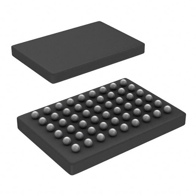
This IC is packaged in a 56-pin VQFN (Very Thin Quad Flat No-Lead) package. Each package contains one unit of the 74CBTLV16211CGRDR.
Specifications
- Supply Voltage Range: 1.65V to 3.6V
- Input/Output Voltage Range: GND to VCC
- Operating Temperature Range: -40°C to +85°C
- Maximum Input Current: ±10mA
- Maximum Output Current: ±32mA
- Propagation Delay: <5ns
- On-Resistance: <10Ω
Pin Configuration
The 74CBTLV16211CGRDR features a total of 56 pins, each serving a specific function. The detailed pin configuration is as follows:
- A0
- A1
- A2
- A3
- A4
- A5
- A6
- A7
- A8
- A9
- A10
- A11
- A12
- A13
- A14
- A15
- OE#
- I/O0
- I/O1
- I/O2
- I/O3
- I/O4
- I/O5
- I/O6
- I/O7
- I/O8
- I/O9
- I/O10
- I/O11
- I/O12
- I/O13
- I/O14
- I/O15
- VCC
- GND
- B0
- B1
- B2
- B3
- B4
- B5
- B6
- B7
- B8
- B9
- B10
- B11
- B12
- B13
- B14
- B15
- OE#
- I/O16
- I/O17
- I/O18
- I/O19
Functional Features
The 74CBTLV16211CGRDR offers the following functional features:
- Bidirectional signal routing: It allows for bidirectional data transmission, enabling seamless communication between multiple input and output channels.
- Low power consumption: The IC is designed to minimize power consumption, making it suitable for battery-powered devices and energy-efficient applications.
- ESD protection: The device incorporates built-in electrostatic discharge (ESD) protection, safeguarding against potential damage caused by static electricity.
- High-speed switching: With its fast propagation delay and low on-resistance, the IC ensures rapid signal switching, enhancing overall system performance.
Advantages and Disadvantages
Advantages
- Low voltage operation for compatibility with modern electronic systems.
- Compact package size for space-efficient integration.
- Wide operating temperature range for versatility in various environments.
- Fast switching times for minimal signal delay.
- Built-in ESD protection for enhanced reliability.
Disadvantages
- Limited number of input/output channels (20 in total).
- May require additional external components for specific applications.
Working Principles
The 74CBTLV16211CGRDR operates based on the principles of multiplexing and demultiplexing. It utilizes a combination of digital logic gates and transistors to selectively route signals between multiple inputs and outputs. By controlling the appropriate control signals, the IC can direct data flow in different configurations, enabling efficient data selection and routing.
Application Field Plans
The
Senaraikan 10 soalan dan jawapan biasa yang berkaitan dengan aplikasi 74CBTLV16211CGRDR dalam penyelesaian teknikal
Sure! Here are 10 common questions and answers related to the application of 74CBTLV16211CGRDR in technical solutions:
Q: What is the 74CBTLV16211CGRDR? A: The 74CBTLV16211CGRDR is a high-speed, low-power 24-bit bus switch with 5V tolerant inputs and outputs.
Q: What is the purpose of the 74CBTLV16211CGRDR? A: It is designed to provide bidirectional voltage level translation between different logic levels, making it useful for interfacing between devices operating at different voltage levels.
Q: What voltage levels does the 74CBTLV16211CGRDR support? A: It supports voltage translation between 1.2V and 3.6V on the A port and 1.65V to 5.5V on the B port.
Q: How many channels does the 74CBTLV16211CGRDR have? A: It has 24 channels, allowing for simultaneous bidirectional translation of 24 signals.
Q: What is the maximum data rate supported by the 74CBTLV16211CGRDR? A: It can support data rates up to 400 Mbps, making it suitable for high-speed applications.
Q: Can the 74CBTLV16211CGRDR be used as a level shifter? A: Yes, it can be used as a level shifter to convert signals between different voltage domains.
Q: Does the 74CBTLV16211CGRDR have any built-in ESD protection? A: Yes, it has built-in ESD protection, which helps safeguard against electrostatic discharge events.
Q: Can the 74CBTLV16211CGRDR be used in both digital and analog applications? A: No, it is primarily designed for digital applications and may not be suitable for precision analog signals.
Q: What is the power supply voltage range for the 74CBTLV16211CGRDR? A: It operates with a power supply voltage range of 1.2V to 3.6V.
Q: Is the 74CBTLV16211CGRDR available in different package options? A: Yes, it is available in various package options, such as TSSOP and VFBGA, providing flexibility for different PCB layouts and space constraints.
Please note that these answers are general and may vary depending on the specific application and requirements.