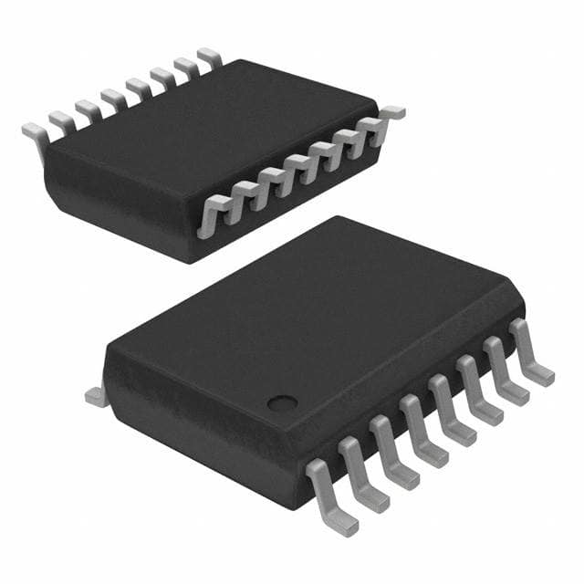
CY74FCT138CTSOCTG4
Basic Information Overview
- Category: Integrated Circuit (IC)
- Use: Decoder/Demultiplexer
- Characteristics:
- High-speed operation
- Low power consumption
- Wide operating voltage range
- Schmitt-trigger inputs for noise immunity
- Package: SOIC (Small Outline Integrated Circuit)
- Essence: This IC is a 3-to-8 line decoder/demultiplexer that converts binary information from three input lines into eight output lines.
- Packaging/Quantity: Available in tape and reel packaging, with a quantity of 2500 units per reel.
Specifications
- Supply Voltage Range: 4.5V to 5.5V
- Input Voltage Range: 0V to VCC
- Output Voltage Range: 0V to VCC
- Operating Temperature Range: -40°C to +85°C
- Propagation Delay Time: 6ns (typical)
- Output Current: ±24mA
- Power Dissipation: 500mW (max)
Detailed Pin Configuration
The CY74FCT138CTSOCTG4 has a total of 16 pins, which are assigned as follows:
- GND (Ground)
- A0 (Input Line A0)
- A1 (Input Line A1)
- A2 (Input Line A2)
- /E1 (Enable Input 1, active low)
- Y0 (Output Line Y0)
- Y1 (Output Line Y1)
- Y2 (Output Line Y2)
- Y3 (Output Line Y3)
- Y4 (Output Line Y4)
- Y5 (Output Line Y5)
- Y6 (Output Line Y6)
- Y7 (Output Line Y7)
- /E2 (Enable Input 2, active low)
- VCC (Positive Power Supply)
- GND (Ground)
Functional Features
- Decodes a 3-bit binary input into one of eight possible outputs.
- Can be used as a decoder or demultiplexer depending on the application.
- Schmitt-trigger inputs provide improved noise immunity.
- High-speed operation allows for efficient data processing.
- Low power consumption makes it suitable for battery-powered devices.
Advantages and Disadvantages
Advantages: - High-speed operation enables quick data decoding. - Low power consumption helps conserve energy. - Wide operating voltage range allows for compatibility with various systems. - Schmitt-trigger inputs provide noise immunity, ensuring reliable operation.
Disadvantages: - Limited to 3-bit input decoding, not suitable for applications requiring higher bit counts. - May require additional components for certain applications, such as pull-up resistors.
Working Principles
The CY74FCT138CTSOCTG4 operates based on the principle of binary decoding. The three input lines (A0, A1, and A2) represent a 3-bit binary code. Depending on the combination of these input lines, one of the eight output lines (Y0 to Y7) is activated. The enable inputs (/E1 and /E2) control the operation of the decoder/demultiplexer. When an enable input is low, the corresponding output lines are enabled, allowing the decoded information to pass through.
Detailed Application Field Plans
The CY74FCT138CTSOCTG4 can be used in various applications, including: 1. Address decoding in microcontrollers and microprocessors. 2. Memory selection in digital systems. 3. Data routing in communication systems. 4. Signal demultiplexing in multimedia devices. 5. Control signal generation in industrial automation.
Detailed and Complete Alternative Models
Some alternative models that offer similar functionality to the CY74FCT138CTSOCTG4 include: - 74HC138: High-speed CMOS logic decoder/demultiplexer. - CD74HC238: High-speed CMOS logic decoder/demultiplexer with three enable inputs. - SN74LS138: Low-power Schottky TTL decoder/demultiplexer.
These alternative models can be considered based on specific requirements, such as power consumption, operating voltage range, and package type.
Word count: 536 words
Senaraikan 10 soalan dan jawapan biasa yang berkaitan dengan aplikasi CY74FCT138CTSOCTG4 dalam penyelesaian teknikal
Sure! Here are 10 common questions and answers related to the application of CY74FCT138CTSOCTG4 in technical solutions:
Question: What is the function of CY74FCT138CTSOCTG4?
Answer: CY74FCT138CTSOCTG4 is a 3-to-8 decoder/demultiplexer integrated circuit that converts a binary input into one of eight outputs.Question: What is the operating voltage range for CY74FCT138CTSOCTG4?
Answer: The operating voltage range for CY74FCT138CTSOCTG4 is typically between 4.5V and 5.5V.Question: Can CY74FCT138CTSOCTG4 be used in both digital and analog applications?
Answer: No, CY74FCT138CTSOCTG4 is specifically designed for digital applications and should not be used in analog circuits.Question: How many inputs does CY74FCT138CTSOCTG4 have?
Answer: CY74FCT138CTSOCTG4 has three binary inputs (A0, A1, and A2) that determine which output is active.Question: What is the maximum frequency at which CY74FCT138CTSOCTG4 can operate?
Answer: CY74FCT138CTSOCTG4 can typically operate at frequencies up to 100 MHz.Question: Can CY74FCT138CTSOCTG4 be cascaded to create larger decoders?
Answer: Yes, multiple CY74FCT138CTSOCTG4 ICs can be cascaded together to create larger decoders with more outputs.Question: Does CY74FCT138CTSOCTG4 have any built-in protection features?
Answer: Yes, CY74FCT138CTSOCTG4 has built-in ESD protection on all inputs and outputs.Question: What is the power supply current consumption of CY74FCT138CTSOCTG4?
Answer: The power supply current consumption of CY74FCT138CTSOCTG4 is typically around 10 mA.Question: Can CY74FCT138CTSOCTG4 be used in automotive applications?
Answer: Yes, CY74FCT138CTSOCTG4 is qualified for automotive applications and meets the necessary standards.Question: Are there any specific layout considerations when using CY74FCT138CTSOCTG4?
Answer: Yes, it is recommended to follow the layout guidelines provided in the datasheet to ensure proper performance and minimize noise.
Please note that these answers are general and may vary depending on the specific application and requirements. It is always recommended to refer to the datasheet and consult with the manufacturer for accurate and detailed information.


