

MSC1210Y3PAGT
Product Overview
- Category: Integrated Circuit (IC)
- Use: Analog-to-Digital Converter (ADC)
- Characteristics: High-resolution, low-power consumption
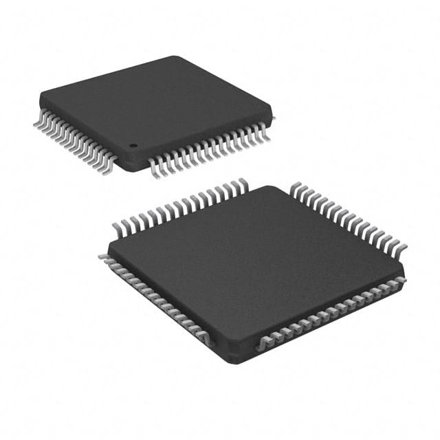
- Package: 20-pin TSSOP (Thin Shrink Small Outline Package)
- Essence: Conversion of analog signals to digital data
- Packaging/Quantity: Tape and reel packaging, 250 units per reel
Specifications
- Resolution: 12 bits
- Sampling Rate: 100 kilosamples per second (ksps)
- Input Voltage Range: 0 to Vref
- Power Supply: 2.7V to 5.5V
- Operating Temperature Range: -40°C to +85°C
Detailed Pin Configuration
- VDD: Power supply voltage
- AGND: Analog ground
- REF: Reference voltage input
- VREFOUT: Buffered reference voltage output
- VIN: Analog input voltage
- VSS: Ground
- D0-D11: Digital output pins
- CS: Chip select input
- SCLK: Serial clock input
- SDI: Serial data input
- SDO: Serial data output
- EOC: End of conversion output
- DGND: Digital ground
- CLKOUT: Clock output
- MCLK: Master clock input
- RESET: Reset input
- TEST: Test mode input
- NC: No connection
- NC: No connection
- NC: No connection
Functional Features
- High-resolution ADC with 12-bit resolution
- Low-power consumption for energy-efficient applications
- Wide operating voltage range allows flexibility in power supply selection
- Fast sampling rate of 100 ksps enables real-time data acquisition
- Buffered reference voltage output for accurate conversions
- End of conversion output signal for synchronization with external devices
Advantages and Disadvantages
Advantages
- High resolution provides precise measurement capabilities
- Low-power consumption extends battery life in portable devices
- Wide operating voltage range allows compatibility with various systems
- Fast sampling rate enables real-time data acquisition
- Buffered reference voltage output ensures accurate conversions
Disadvantages
- Limited number of digital output pins may restrict the number of connected devices
- 20-pin package may not be suitable for space-constrained applications
Working Principles
The MSC1210Y3PAGT is an analog-to-digital converter that converts analog signals into digital data. It operates by sampling the input voltage and converting it into a binary representation using a 12-bit resolution. The conversion process is controlled by the internal clock and can be triggered by the chip select input. The converted digital data is then available at the digital output pins for further processing or storage.
Detailed Application Field Plans
The MSC1210Y3PAGT is widely used in various applications that require high-resolution analog-to-digital conversion. Some potential application fields include:
- Industrial Automation: Precise measurement and control systems
- Medical Devices: Biomedical signal acquisition and analysis
- Automotive Electronics: Sensor data acquisition and processing
- Consumer Electronics: Audio signal processing and measurement
- Energy Management: Power monitoring and control systems
Detailed and Complete Alternative Models
- ADC1210HCDT: 12-bit ADC, 8-pin SOIC package
- ADS1220IPWR: 24-bit ADC, 16-pin TSSOP package
- MAX11100PMB1: 16-bit ADC, evaluation board
- LTC1867LIGN: 16-bit ADC, 16-pin SSOP package
- MCP3208-CI/P: 12-bit ADC, 16-pin DIP package
These alternative models offer different resolutions, package options, and features to suit specific application requirements.
Word count: 446 words
Senaraikan 10 soalan dan jawapan biasa yang berkaitan dengan aplikasi MSC1210Y3PAGT dalam penyelesaian teknikal
Sure! Here are 10 common questions and answers related to the application of MSC1210Y3PAGT in technical solutions:
Q: What is the MSC1210Y3PAGT? A: The MSC1210Y3PAGT is a microcontroller unit (MCU) manufactured by Texas Instruments, commonly used in technical solutions.
Q: What are the key features of the MSC1210Y3PAGT? A: The key features include an integrated analog-to-digital converter (ADC), digital-to-analog converter (DAC), on-chip memory, serial communication interfaces, and various peripherals.
Q: How can the MSC1210Y3PAGT be used in technical solutions? A: It can be used for data acquisition, control systems, sensor interfacing, signal processing, and other applications that require embedded computing capabilities.
Q: What programming language is used to program the MSC1210Y3PAGT? A: The MSC1210Y3PAGT can be programmed using assembly language or high-level languages like C.
Q: Can the MSC1210Y3PAGT interface with external sensors? A: Yes, it has built-in ADCs and DACs that allow it to interface with various analog sensors and actuators.
Q: Does the MSC1210Y3PAGT support communication protocols like I2C or SPI? A: Yes, it supports popular communication protocols like I2C, SPI, UART, and CAN, making it versatile for connecting with other devices.
Q: What is the power supply requirement for the MSC1210Y3PAGT? A: The typical operating voltage range is 2.7V to 5.5V, but it is recommended to refer to the datasheet for specific details.
Q: Can the MSC1210Y3PAGT be used in battery-powered applications? A: Yes, it has low power consumption capabilities and can be used in battery-powered applications with proper power management techniques.
Q: Are there any development tools available for programming the MSC1210Y3PAGT? A: Yes, Texas Instruments provides development tools like compilers, debuggers, and evaluation boards specifically designed for programming and testing the MSC1210Y3PAGT.
Q: Where can I find additional resources and documentation for the MSC1210Y3PAGT? A: You can find detailed datasheets, application notes, reference designs, and other resources on the Texas Instruments website or by contacting their technical support team.