

SN74AHCT138DGVR
Product Overview
- Category: Integrated Circuit (IC)
- Use: Decoder/Demultiplexer
- Characteristics: High-speed, low-power, 3-to-8 line decoder/demultiplexer
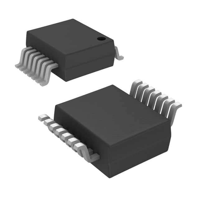
- Package: VSSOP-16
- Essence: Converts a binary input into a corresponding output based on the selected line
- Packaging/Quantity: Tape and Reel, 2500 units per reel
Specifications
- Supply Voltage Range: 2V to 5.5V
- Input Voltage Range: 0V to VCC
- Output Voltage Range: 0V to VCC
- Maximum Operating Frequency: 50 MHz
- Low Power Consumption: ICC = 4µA (Max)
- High Noise Immunity: VNIH = VNIL = 28% VCC (Min)
Detailed Pin Configuration
The SN74AHCT138DGVR has a total of 16 pins, each serving a specific purpose:
- GND: Ground
- A0: Address Input 0
- A1: Address Input 1
- A2: Address Input 2
- E1: Enable Input 1
- Y0: Output 0
- Y1: Output 1
- Y2: Output 2
- Y3: Output 3
- Y4: Output 4
- Y5: Output 5
- Y6: Output 6
- Y7: Output 7
- E2: Enable Input 2
- VCC: Positive Power Supply
- GND: Ground
Functional Features
The SN74AHCT138DGVR is designed to decode a three-bit binary input and generate eight mutually exclusive outputs. It operates at high speed while consuming low power, making it suitable for various applications. The decoder/demultiplexer has two enable inputs (E1 and E2) that can be used to activate or deactivate the outputs based on specific conditions.
Advantages and Disadvantages
Advantages: - High-speed operation - Low power consumption - Wide supply voltage range - High noise immunity
Disadvantages: - Limited number of input lines - Only supports binary inputs
Working Principles
The SN74AHCT138DGVR works by accepting a three-bit binary input (A0, A1, A2) and decoding it into one of the eight output lines (Y0-Y7). The enable inputs (E1 and E2) control the activation of the outputs. When both enable inputs are high, all outputs are active. By manipulating the address inputs, specific output lines can be selected.
Detailed Application Field Plans
The SN74AHCT138DGVR is commonly used in various digital systems where decoding and demultiplexing functions are required. Some typical application fields include:
- Address Decoding: Used in microprocessors and memory systems to decode memory addresses.
- Data Demultiplexing: Used to route data from a single source to multiple destinations.
- Control Signal Generation: Used to generate control signals for different components in a system.
- Display Multiplexing: Used in multiplexed display systems to select specific segments or digits.
Detailed and Complete Alternative Models
- 74HC138: Similar functionality but operates at a higher voltage range (2V to 6V).
- CD74HCT138: Compatible alternative with similar specifications and pin configuration.
- SN54AHCT138: Equivalent model with wider temperature range (-55°C to 125°C).
These alternative models provide similar decoding and demultiplexing capabilities, allowing users to choose the most suitable option based on their specific requirements.
Word count: 409 words
Senaraikan 10 soalan dan jawapan biasa yang berkaitan dengan aplikasi SN74AHCT138DGVR dalam penyelesaian teknikal
Sure! Here are 10 common questions and answers related to the application of SN74AHCT138DGVR:
Q: What is the SN74AHCT138DGVR? A: The SN74AHCT138DGVR is a 3-to-8 line decoder/demultiplexer integrated circuit (IC) commonly used in digital electronics.
Q: What is the purpose of the SN74AHCT138DGVR? A: The purpose of this IC is to decode a binary input and activate one of the eight output lines based on the input value.
Q: What is the voltage range supported by the SN74AHCT138DGVR? A: The SN74AHCT138DGVR supports a voltage range of 4.5V to 5.5V.
Q: How many inputs does the SN74AHCT138DGVR have? A: The SN74AHCT138DGVR has three inputs, namely A0, A1, and A2.
Q: How many output lines does the SN74AHCT138DGVR have? A: The SN74AHCT138DGVR has eight output lines, labeled Y0 to Y7.
Q: Can the SN74AHCT138DGVR be cascaded to increase the number of outputs? A: Yes, multiple SN74AHCT138DGVR ICs can be cascaded together to increase the number of outputs.
Q: What is the maximum current that each output line of the SN74AHCT138DGVR can sink/source? A: Each output line of the SN74AHCT138DGVR can sink/source up to 8mA of current.
Q: Is the SN74AHCT138DGVR compatible with TTL logic levels? A: Yes, the SN74AHCT138DGVR is compatible with both TTL and CMOS logic levels.
Q: Can the SN74AHCT138DGVR be used in both active-high and active-low configurations? A: Yes, the SN74AHCT138DGVR can be used in both active-high and active-low configurations depending on the input values.
Q: What are some common applications of the SN74AHCT138DGVR? A: The SN74AHCT138DGVR is commonly used in address decoding, memory selection, data routing, and general-purpose digital logic circuits.
Please note that these answers are general and may vary based on specific design requirements and datasheet specifications.