

SN74ALVCH245DGVR
Basic Information Overview
- Category: Integrated Circuit (IC)
- Use: Level Shifter and Bus Transceiver
- Characteristics: Bi-directional voltage level translation, low power consumption, high-speed operation
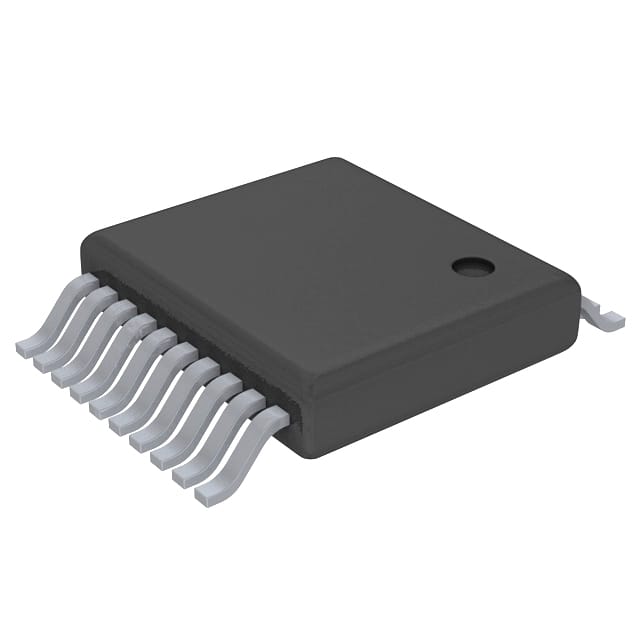
- Package: TSSOP-20
- Essence: This IC is designed to provide bidirectional voltage level translation between different logic levels in electronic circuits.
- Packaging/Quantity: Available in tape and reel packaging, with 2500 units per reel.
Specifications
- Supply Voltage Range: 1.65V to 3.6V
- Logic Voltage Levels: 1.8V, 2.5V, 3.3V
- Maximum Data Rate: 400 Mbps
- Number of Channels: 8
- Input/Output Type: Tri-State
- Operating Temperature Range: -40°C to +85°C
Detailed Pin Configuration
The SN74ALVCH245DGVR has a total of 20 pins, which are assigned as follows:
- OE (Output Enable) 1
- A1 (Data Input/Output) 1
- B1 (Data Input/Output) 1
- A2 (Data Input/Output) 2
- B2 (Data Input/Output) 2
- A3 (Data Input/Output) 3
- B3 (Data Input/Output) 3
- GND (Ground)
- B4 (Data Input/Output) 4
- A4 (Data Input/Output) 4
- B5 (Data Input/Output) 5
- A5 (Data Input/Output) 5
- B6 (Data Input/Output) 6
- A6 (Data Input/Output) 6
- B7 (Data Input/Output) 7
- A7 (Data Input/Output) 7
- VCC (Power Supply)
- B8 (Data Input/Output) 8
- A8 (Data Input/Output) 8
- OE (Output Enable) 2
Functional Features
- Bi-directional voltage level translation: Allows seamless communication between circuits operating at different logic levels.
- Tri-State outputs: Enables multiple devices to share a common bus without interfering with each other.
- Low power consumption: Helps conserve energy in battery-powered applications.
- High-speed operation: Supports fast data transfer rates up to 400 Mbps.
Advantages and Disadvantages
Advantages: - Efficient voltage level translation between different logic levels. - Tri-State outputs allow for bus sharing. - Low power consumption extends battery life. - High-speed operation enables rapid data transfer.
Disadvantages: - Limited to specific logic voltage levels (1.8V, 2.5V, 3.3V). - May not be suitable for applications requiring voltage translation beyond the specified range.
Working Principles
The SN74ALVCH245DGVR operates by receiving input signals from one logic level and translating them to another logic level. It uses a combination of MOSFETs and CMOS technology to achieve bidirectional voltage level translation. The Output Enable (OE) pins control the direction of data flow, allowing the IC to function as both a level shifter and a bus transceiver.
Detailed Application Field Plans
The SN74ALVCH245DGVR is commonly used in various electronic systems where voltage level translation is required. Some typical application fields include: - Microcontroller interfacing with different logic families. - Communication interfaces between devices operating at different voltage levels. - Bus transceivers in computer systems and networking equipment. - Level shifting in battery-powered portable devices.
Detailed and Complete Alternative Models
- SN74LVC245A: Similar functionality with a wider supply voltage range (1.65V to 5.5V).
- SN74LVCH245A: Improved speed performance with a maximum data rate of 500 Mbps.
- SN74AVC4T245: Four-channel level shifter with integrated voltage translation and direction control.
These alternative models offer similar features and can be considered based on specific application requirements.
Word count: 431 words
Senaraikan 10 soalan dan jawapan biasa yang berkaitan dengan aplikasi SN74ALVCH245DGVR dalam penyelesaian teknikal
Sure! Here are 10 common questions and answers related to the application of SN74ALVCH245DGVR:
Q: What is SN74ALVCH245DGVR? A: SN74ALVCH245DGVR is a bidirectional octal bus transceiver with 3-state outputs, commonly used in digital systems.
Q: What is the voltage range supported by SN74ALVCH245DGVR? A: SN74ALVCH245DGVR supports a voltage range of 1.65V to 3.6V.
Q: How many channels does SN74ALVCH245DGVR have? A: SN74ALVCH245DGVR has 8 bidirectional channels.
Q: Can SN74ALVCH245DGVR be used for level shifting? A: Yes, SN74ALVCH245DGVR can be used for level shifting between different voltage domains.
Q: What is the maximum data transfer rate supported by SN74ALVCH245DGVR? A: SN74ALVCH245DGVR supports a maximum data transfer rate of 400 Mbps.
Q: Does SN74ALVCH245DGVR have built-in ESD protection? A: Yes, SN74ALVCH245DGVR has built-in ESD protection on all pins.
Q: Can SN74ALVCH245DGVR be used in both input and output applications? A: Yes, SN74ALVCH245DGVR can be used as both an input and output buffer.
Q: What is the power supply voltage required for SN74ALVCH245DGVR? A: SN74ALVCH245DGVR requires a power supply voltage of 1.65V to 3.6V.
Q: Can SN74ALVCH245DGVR be used in high-speed applications? A: Yes, SN74ALVCH245DGVR is suitable for high-speed applications due to its low propagation delay.
Q: Is SN74ALVCH245DGVR compatible with other logic families? A: Yes, SN74ALVCH245DGVR is compatible with a wide range of logic families, including TTL, CMOS, and LVCMOS.
Please note that these answers are general and may vary depending on specific application requirements.